

Industrial Pcb production runs follow predictable patterns from initial design handover through final delivery. Understanding this lifecycle helps engineers, project managers, and hardware teams plan effectively, set realistic expectations, and troubleshoot issues when they arise. Each stage of the production process builds upon previous steps, creating dependencies that require careful coordination.
This guide walks through the complete production lifecycle, explaining what happens at each stage, typical timelines, and factors that influence duration and quality. Whether you are new to Electronics Manufacturing or seeking to optimize existing processes, this knowledge helps you navigate production runs more effectively.

Every production run begins when design files reach the manufacturer. This stage sets the foundation for everything that follows. The quality and completeness of handover documentation directly impacts production efficiency, yield rates, and time-to-delivery. Engineers should approach handover preparation with the same rigor applied to original design work.
Design handover typically includes Gerber files for each board layer, drill files, Solder Mask specifications, Silkscreen artwork, and BOM (bill of materials). Each file type serves specific manufacturing purposes, and missing or incorrect files delay production while manufacturers request corrections.
Upon receiving design files, manufacturers conduct Design For Manufacturing analysis. This review identifies potential production issues before fabrication begins. Common concerns include trace widths too narrow for reliable etching, via sizes incompatible with drilling capabilities, and spacing violations that risk solder bridging during assembly.
DFM feedback typically arrives within 24-72 hours for standard complexity boards. Simple designs may receive clearance quickly, while complex multilayer boards with fine features require more extensive analysis. Manufacturers should communicate identified issues clearly and propose specific corrections that designers can implement.
Beyond DFM analysis, manufacturers assess whether their equipment and processes can meet design requirements. This feasibility check verifies that specified materials are available, that layer counts and stackup requirements fall within manufacturing capabilities, and that specialized processes like blind/buried vias are supported.
Feasibility assessment may identify constraints that require design modification. These constraints often surface as minimum feature sizes, maximum layer counts, or material availability issues. Resolving feasibility concerns before production prevents delays and avoids costly rework after fabrication begins.
The design handover stage typically spans 2-5 business days, depending on design complexity and manufacturer responsiveness. Complex multilayer boards with advanced features may require longer engineering review. Simple two-layer boards often clear review within 1-2 days.
Design teams should anticipate potential revision cycles if DFM feedback requires changes. Building buffer time into project schedules accounts for this possibility. Early engagement with manufacturers during design, rather than just at handover, reduces revision cycles by addressing concerns while design changes remain easy to implement.
Once designs pass review, manufacturers begin procuring materials and setting up production tooling. This stage transitions from engineering preparation to physical manufacturing infrastructure. Lead times for materials and tooling often dominate this stage's duration.
Material procurement encompasses base laminates, copper foil, prepreg, Solder Mask, and surface finish chemicals. Some materials have significant lead times, particularly specialized laminates for high-frequency or high-temperature applications. Manufacturers must balance inventory carrying costs against material availability when stocking for anticipated production.
Material Selection impacts electrical performance, thermal characteristics, and manufacturing compatibility. Standard FR-4 materials offer broad availability and competitive pricing. High-performance materials like High-tg Fr-4, Rogers, or polyimide require longer procurement cycles and may command premium pricing.
Manufacturers maintain relationships with laminate suppliers that provide priority access and faster delivery for common materials. For specialized substrates, procurement may require 2-4 weeks for material delivery alone. Design teams specifying unusual materials should verify availability and factor procurement time into schedules.
PCB Fabrication requires tooling that must be prepared for each unique design. Tooling includes drilling programs, imaging artwork, lamination presses, and cutting dies. Setting up this tooling requires engineering time and machine capacity that manufacturers must schedule.
For multilayer boards, inner layer registration, lamination stackup, and drilling alignment require precise setup. These processes consume significant time before actual board production begins. The setup time exists regardless of order quantity, which is why small prototype runs cost similar amounts to first articles of larger production batches.
For turnkey assembly services, component procurement occurs alongside PCB Fabrication. This parallel activity helps compress overall timelines but requires careful coordination. Component lead times often exceed Pcb Fabrication time, making component availability the critical path for total delivery.
Turnkey manufacturers maintain component inventory for common parts but must source design-specific components for each unique BOM. Long-lead components like specialized ICs or custom magnetics can dominate procurement timelines. Design teams should identify these components early and work with manufacturers to secure availability before production scheduling.
Pcb Fabrication transforms raw materials into completed bare boards. This stage encompasses multiple processes that build the board layer by layer, creating the electrical pathways that will eventually connect components. Fabrication quality directly impacts assembly yield and final product reliability.
Modern PCB fabrication uses automated processes that achieve consistency across production runs. However, each design requires specific machine setups, making rapid design changes challenging during active production. Understanding fabrication processes helps design teams create boards that manufacture reliably.
Multilayer boards begin with inner layer fabrication. Copper-clad laminate receives imaging, where photoresist applied to the copper surface exposes through artwork film. Exposed copper etches away, leaving the designed trace pattern. This process repeats for each inner layer.
After etching, inner layers undergo optical inspection to detect defects. Automated Optical Inspection systems compare fabricated layers against design data, identifying opens, shorts, and dimensional issues. Layers passing inspection proceed to lamination; those with defects may require rework or scrapping.
Multilayer boards stack inner layers with prepreg insulating material and outer copper foil. Heat and pressure bond these materials into unified panels. The lamination process requires precise control of temperature, pressure, and timing to achieve proper dielectric bonding without damaging inner layer features.
Via formation creates electrical connections between layers. Through-hole vias drill through the complete panel stack. Blind Vias connect outer layers to inner layers without penetrating the full stack. Buried vias connect inner layers without reaching surfaces. Each via type requires specific drilling and plating processes.
After lamination, outer layers receive the same imaging and etching processes as inner layers. Surface finish application follows, protecting exposed copper from oxidation while preparing pads for solder attachment. Common finishes include HASL, ENIG, OSP, and immersion silver, each with specific application processes.
Final steps include solder mask application, Silkscreen legend printing, and electrical testing. Automated testing verifies continuity and isolation across the complete board network. Boards passing all tests proceed to depanelization, where individual boards separate from production panels.
Quality inspection occurs throughout fabrication, not just at final output. Each process step includes inspection or testing that catches defects early before additional value adds. This staged inspection approach reduces waste by identifying problems before materials and labor accumulate through subsequent processes.
Final inspection typically includes visual verification, automated electrical testing, and sometimes cross-section analysis for critical features. Manufacturers maintain defect databases that track issues across production runs, enabling Continuous Improvement in process control. Customers should request defect data when troubleshooting field failures.
PCB assembly attaches components to fabricated boards, creating functional electronic circuits. This stage transforms bare boards into populated assemblies ready for testing. Assembly quality depends on component quality, solder joint formation, and process control throughout the assembly sequence.
Surface mount technology dominates modern assembly, though through-hole components remain necessary for certain applications. The assembly process for each technology involves distinct equipment and process parameters, creating complexity when boards include both technologies.
Surface Mount Assembly begins with solder paste application. A stencil, precisely machined to match pad geometry, aligns with the board and deposits solder paste in exact locations. Stencil quality, alignment precision, and paste freshness directly impact solder joint quality downstream.
Solder paste inspection following printing detects insufficient paste, excess paste, or misalignment before components place. This early inspection catches defects that would otherwise require rework after reflow. Manufacturers investing in paste inspection achieve higher first-pass yields than those relying solely on downstream inspection.
Pick-and-place machines position components on boards with sub-millimeter accuracy. Modern placement systems use vision systems to verify component orientation and detect damaged parts before placement. Placement accuracy matters most for fine-pitch components like 0.4mm pitch BGAs, where positional errors cause immediate defects.
Placement speed varies by component type and board density. Complex boards with thousands of components may require extended placement time even on high-speed lines. Placement programs require setup and optimization that add to tooling costs for first production runs of new designs.
Reflow soldering melts solder paste to form permanent connections between components and pads. Controlled heating profiles ensure proper solder melting and wetting while preventing thermal damage to components or boards. Profile optimization for specific board configurations ensures consistent results across production batches.
Post-reflow inspection typically uses Automated Optical Inspection to detect component placement issues and obvious solder defects. For boards with hidden solder joints beneath BGAs or QFNs, X-ray inspection reveals defects invisible to optical systems. Manufacturers should match inspection methods to board complexity and defect risk.
Boards including through-hole components require additional assembly processes. Wave Soldering immerses boards in molten solder, forming connections on component leads passing through holes. Selective Soldering addresses specific through-hole connections without affecting nearby surface mount components.
Hand soldering remains necessary for some through-hole components, particularly those with thermal sensitivity or unusual form factors. Hand assembly introduces variability that automated processes avoid, making statistical process control challenging. Design teams should minimize through-hole content when assembly efficiency matters.
Testing verifies that assembled boards function correctly and meet quality specifications. Comprehensive testing catches defects before boards reach customers, reducing field failures and warranty costs. Testing strategies should match board complexity and application criticality.
Different test approaches address different defect types. In-circuit testing verifies individual component placement and solder integrity. Functional Testing validates that boards perform intended operations. Boundary Scan testing accesses digital circuits through JTAG interfaces. Each method contributes to overall quality confidence.
In-circuit testing applies electrical signals to boards while components remain unpowered. The test system verifies component presence, values, and solder joint integrity by measuring resistance, capacitance, and voltage at Test Points. Ict typically achieves high defect detection rates for manufacturing defects.
Ict requires test fixtures with spring-loaded probes that contact board Test Points. Fixture construction adds cost and lead time to first production runs. For low-volume or prototype production, Flying Probe Testing offers fixture-free alternative at slower test speeds. Flying probe suits development-stage boards where test point definitions may evolve.
Functional Testing applies power and signals to boards, verifying correct operation under realistic conditions. Unlike ICT which tests individual nodes, functional test exercises complete board behavior. This testing catches defects that ICT misses, including Design Errors, component interactions, and subtle manufacturing issues affecting performance.
Functional test programs require development for each unique board design. Test development takes time and expertise, adding to production costs particularly for first articles. The investment pays dividends through ongoing defect detection throughout production. Test programs should include stress conditions that accelerate latent defect discovery.
For high-reliability applications, boards may undergo burn-in or environmental stress testing. Burn-in operates boards at elevated temperature and voltage, accelerating failure mechanisms that would otherwise appear in early field service. Environmental Testing exposes boards to temperature cycling, humidity, vibration, and other stress factors.
Stress testing requires extended time and environmental chamber capacity. The investment identifies infant mortality defects before customer delivery, improving field reliability for critical applications. Not all products require stress testing, but designs for aerospace, medical, or automotive applications typically do.
Boards passing testing proceed to finishing operations and packaging. This stage prepares boards for storage and shipment while protecting against damage during transit. Proper finishing and packaging maintains quality achieved through earlier production stages.
Finishing operations may include Conformal Coating for boards requiring moisture or contamination protection. Some assemblies receive potting or encapsulation for extreme environmental protection. Programming and configuration operations also occur at this stage for boards requiring firmware or calibration data.
Conformal Coating applies thin polymer films that conform to board topography, providing barrier protection against moisture, dust, and contaminants. Common coatings include acrylic, silicone, urethane, and parylene, each with specific application methods and performance characteristics.
Coating application requires masking connectors and other components that should not receive coverage. Application processes include spraying, dipping, and selective coating. Curing follows application, with some coatings requiring oven curing while others cure at room temperature.
Proper packaging prevents transit damage during storage and shipment. ESD-sensitive boards require static-protective packaging throughout. Fragile components may require additional cushioning. Boards intended for automated assembly often receive tray or tube packaging compatible with pick-and-place equipment.
Packaging specifications should match anticipated storage conditions and transit hazards. Extended storage before installation requires enhanced Moisture Protection. International shipment may require specific packaging to comply with customs and handling requirements.
Complete documentation accompanies shipments, including test reports, Certificates of Conformance, and traceability records. Test reports document electrical testing results, demonstrating that boards meet specifications. Certificates of Conformance attest to manufacturing processes and quality system compliance.
Traceability records link finished boards to specific production lots of materials and components. This traceability enables Failure Analysis when field issues occur, narrowing investigation scope to specific material lots or process parameters. High-reliability industries typically require formal traceability programs with unique serial numbers for each board.
Manufacturing completion marks transition to delivery and ongoing support. This stage encompasses shipment, receipt inspection, and warranty support. Responsiveness during post-production support often differentiates excellent manufacturers from merely adequate ones.
Delivery logistics may involve domestic shipment or international freight. Lead time for shipment varies by destination and shipping method. Expedited shipping costs significantly more than standard ground freight but may justify the premium for time-critical needs.
Customers should perform receipt inspection to verify delivered boards match requirements. This inspection typically includes visual verification of quantities and markings, electrical testing on sample boards, and dimensional verification against specifications. Receipt inspection catches shipping damage and obvious discrepancies.
Initial qualification testing subjects sample boards to thorough evaluation before full integration or deployment. This qualification may include extended functional testing, Environmental Stress Screening, and Reliability Testing. Qualification results guide acceptance decisions and identify potential issues requiring manufacturer coordination.
Manufacturers typically warrant that delivered boards meet specifications and are free from manufacturing defects. Warranty periods vary by manufacturer and application, commonly spanning 90 days to one year. Warranty coverage may include repair, replacement, or credit depending on issue severity and cause determination.
Failure Analysis when boards do not perform as expected helps determine root cause and appropriate resolution. Professional manufacturers participate actively in failure investigation, providing test data, process records, and engineering analysis. The cooperation level during failure resolution often indicates the relationship quality you can expect ongoing.
Ongoing production benefits from continuous feedback between customers and manufacturers. Defect trends, process improvements, and design optimizations should flow both directions. Manufacturers who engage constructively with feedback improve their service quality over time.
Regular reviews with manufacturing partners surface improvement opportunities and emerging concerns before they become serious problems. Quarterly or annual business reviews provide structured forums for discussing performance, roadmap alignment, and development needs. These relationships improve with investment, often yielding benefits that exceed initial expectations.
Production run timelines vary based on multiple factors, some within designer control and others determined by manufacturer capabilities and external circumstances. Understanding these factors helps set realistic expectations and identify opportunities for timeline compression.
Design complexity typically drives the largest timeline variations. Simple two-layer boards may complete fabrication in days, while complex multilayer boards with advanced features may require weeks. Component availability introduces additional variability that depends on supply chain conditions.
Board complexity scales with layer count, feature density, and specialized requirements. Each additional layer adds fabrication steps and processing time. Fine-line geometries and tight tolerances require additional inspection and may reduce manufacturing yields, extending timelines when reworks occur.
Specialized features like blind/buried vias, impedance control, and heavy copper significantly impact fabrication complexity and timelines. These features should be specified only when required by electrical performance needs, not as design defaults. Simplifying designs where possible compresses timelines and reduces costs.
Component availability increasingly dominates production timelines. Semiconductor shortages persist for many part types, creating lead times measured in weeks or months for some components. Design teams specifying readily available components achieve faster production than those specifying scarce parts.
Turnkey manufacturers help navigate availability challenges through distributor relationships and component inventory. However, the underlying supply constraints affect all market participants. Building component availability checks into design selection criteria helps avoid production delays from obsolete or unavailable parts.
Manufacturer production capacity affects order timing regardless of design complexity. Popular manufacturers may have backlog extending weeks, while less-utilized facilities may offer faster scheduling. Capacity constraints often become more acute during industry upturns when demand exceeds available manufacturing capacity.
Building relationships with manufacturers before urgent needs arise helps secure capacity when needed. Long-term customers typically receive scheduling priority over new accounts. The investment in relationship development pays dividends during tight capacity situations.
The lifecycle of an Industrial Pcb production run encompasses multiple stages, each contributing to final product quality and delivery timing. From design handover through fabrication, assembly, testing, and delivery, understanding what happens at each stage helps teams plan effectively and collaborate productively with manufacturing partners.
Design preparation quality fundamentally shapes production run success. Clear specifications, complete documentation, and design-for-manufacturing consideration reduce revision cycles and improve yields. Engaging manufacturers early, rather than only at handover, surfaces potential issues while design changes remain inexpensive.
Production timelines depend heavily on design complexity, component availability, and manufacturer capacity. Building realistic schedules accounts for these factors, with appropriate buffer for unexpected delays. The most successful hardware programs maintain close coordination with manufacturing partners throughout development, treating production readiness as a shared objective rather than a handover event.
Standard lead times for 4-6 layer boards typically range from 10-15 business days for fabrication plus additional time for assembly if included. Complex multilayer boards with advanced features may require 20-30 days or longer. Component procurement for turnkey orders adds variable time depending on availability.
Design simplification reduces fabrication complexity and timeline. Using standard materials instead of specialty substrates accelerates procurement. Selecting readily available components prevents procurement delays. Working with manufacturers who maintain capacity buffer provides faster scheduling. Early design-for-manufacturing engagement surfaces issues before they delay production.
High-reliability applications typically test 100% of boards. Commercial products may sample test from production runs, accepting boards based on statistical sampling when defect rates prove consistently low. Your test coverage should match application criticality and defect risk assessment.
Address obsolescence proactively through lifetime buys of critical components, design modifications to accept replacement parts, or scheduling production to consume stock before discontinuation. Turnkey manufacturers can advise on obsolescence risks and mitigation strategies based on their supply chain visibility.
Standard documentation includes Certificates of Conformance, test reports, and traceability records. Detailed shipments may include inspection data, first-article inspection reports, and material certifications. Specify documentation requirements in your manufacturing agreement to ensure expectations align.
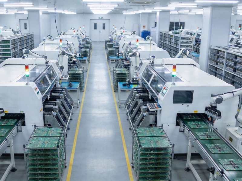
How to Scale Your Industrial PCB Production for Mass ManufacturingJune/02/2026

5 Critical Steps to Optimize Your Industrial PCB Production WorkflowJuly/15/2026
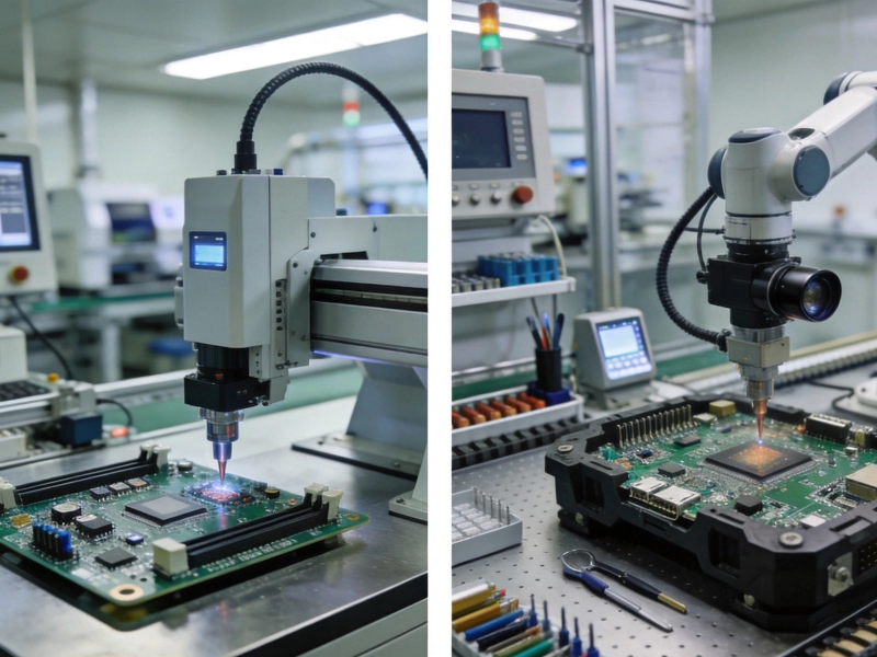
Key Differences Between Consumer and Industrial PCB ProductionJune/27/2026

How Automation is Revolutionizing Industrial PCB Production in 2026September/02/2026

The Complete Guide to Manufacturing Processes and Industry ChallengesMay/27/2026

Cost Analysis: Is Rigid-Flex the Right Solution for Your Industrial Project?September/15/2026
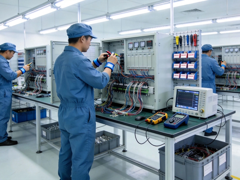
Navigating the Complexities of Box Build AssemblyMay/27/2026

How to Choose the Right Manufacturer for Industrial PCB FabricationJune/29/2026