Open Nav


Every PCB that ships to a customer should work the first time it powers up. Achieving that goal requires more than good design and careful manufacturing—it requires systematic, multi-stage Quality Control testing that catches defects at every stage before they become field failures. In-circuit Test, functional test, and automated optical inspection form the foundation of Industrial Pcb quality assurance. Understanding what each test does, what it catches, and what it misses is essential for anyone responsible for electronics quality.
This guide provides a comprehensive overview of these three critical testing methodologies: how they work, what defects they detect, where they fit in the manufacturing process, and how to build an effective overall test strategy for Industrial Pcb Production.
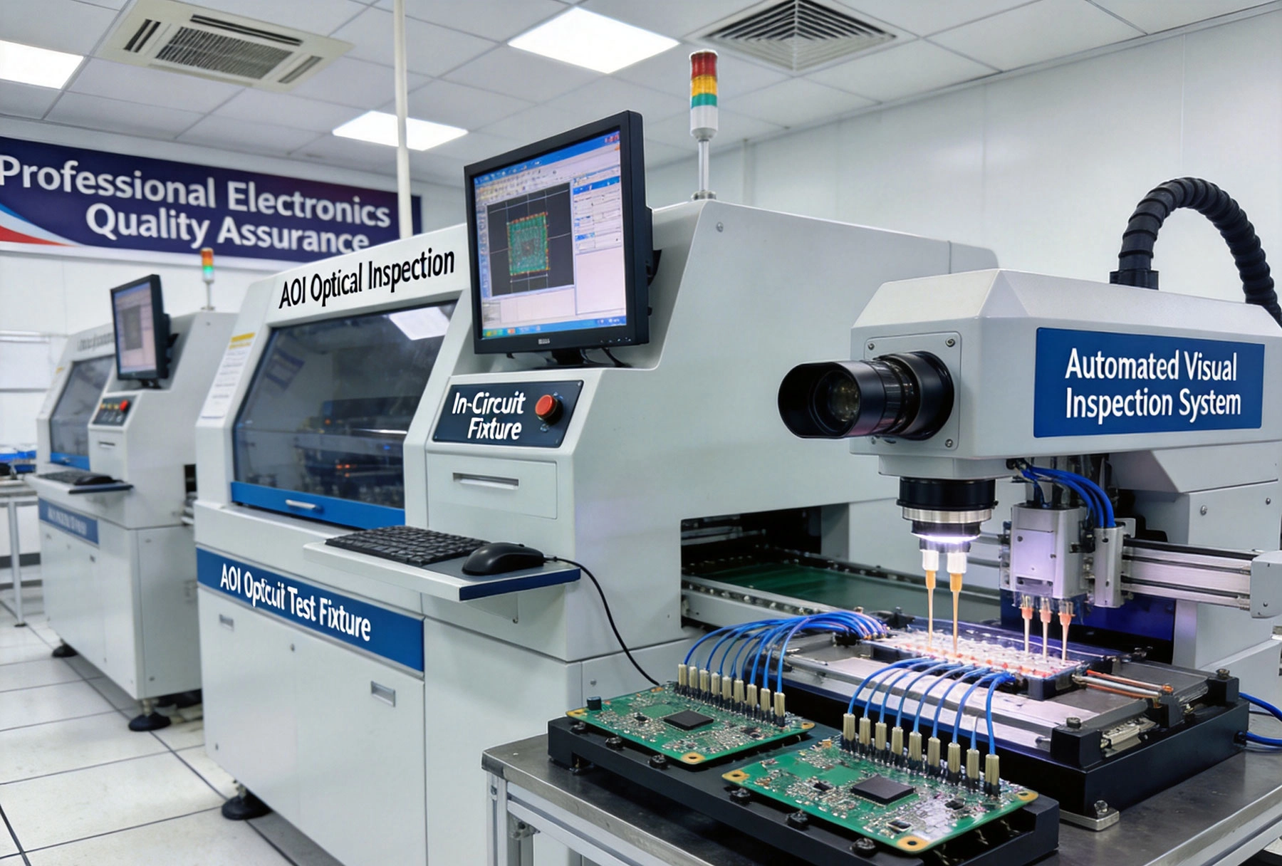
Industrial electronic products operate under conditions that consumer electronics rarely face: temperature extremes, vibration, humidity, long service life requirements, and the expectation of near-zero field failure rates. When an industrial controller fails in a factory, production stops. When a safety system fails, people can be injured. This is why Industrial Pcb manufacturers hold their products to standards that go far beyond basic functionality.
Quality Control testing serves three essential purposes. First, it catches manufacturing defects before products reach customers—defects that would otherwise create warranty costs, customer dissatisfaction, and reputational damage. Second, it provides data that drives Continuous Improvement in the manufacturing process—tracking defect patterns, identifying root causes, and measuring the effectiveness of process changes. Third, it generates the documentation and traceability records that industrial customers increasingly require—proof that the product was built to specification and verified before shipment.
A comprehensive test strategy doesn't rely on any single test method. Each test catches different defect types, and layers of testing provide coverage that no single method can achieve alone.
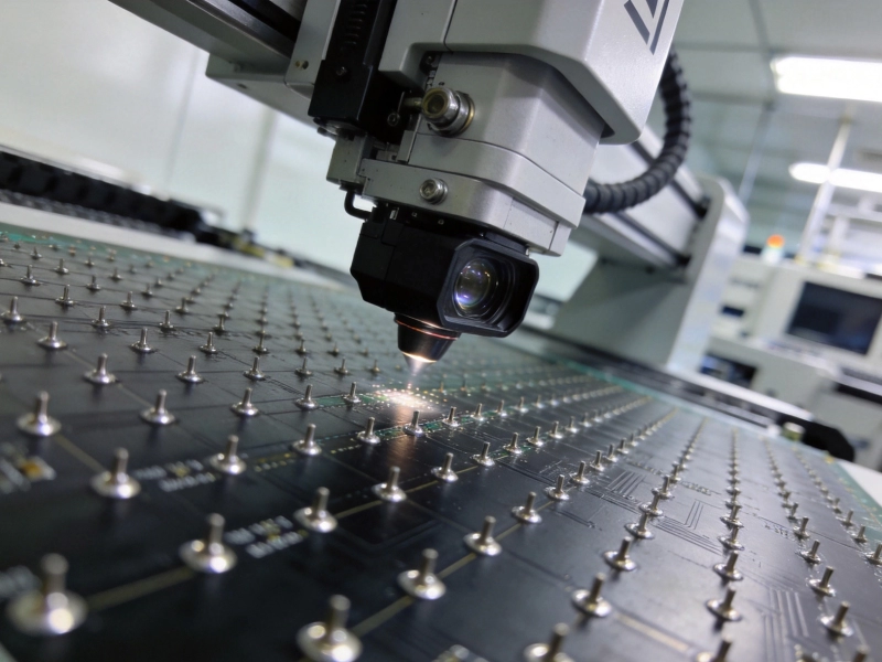
Automated Optical Inspection uses high-resolution cameras and sophisticated image processing software to inspect PCBs for defects in appearance, geometry, and solder quality. Aoi systems image each board from multiple angles, comparing the captured images against the expected board design stored in CAD data. Any deviation from the expected appearance is flagged for operator review.
Modern Aoi systems use structured lighting—multiple light sources at different angles—to create detailed 3D surface maps of the board. This allows detection of defects that would be invisible under uniform lighting: insufficient solder volume, excess solder, component tilt, and lifted leads all create characteristic patterns in the structured light reflection that the software identifies.
AOI excels at detecting defects that are visually apparent:
Component presence and orientation: Missing components, rotated components (e.g., diodes and capacitors installed backwards), and components placed in wrong positions.
Solder defects: Solder bridges (unintended connections between adjacent traces), insufficient solder (cold joints, incomplete wetting), excess solder (solder rollover, icicles), and solder scabs.
Component defects: Component cracking, chipping or lifting from pads, bent leads, and damaged component bodies.
Board defects: Scratches, contamination, lamination defects, and Silkscreen legibility issues.
Lead and terminations: Bent leads, lifted leads, and insufficient lead engagement with solder.
AOI is typically performed after the reflow soldering step—before any through-hole components are installed (if any) and before the board goes to box build. This allows defects to be identified and reworked before the board moves to subsequent assembly stages where rework becomes more expensive and time-consuming. AOI can also be performed after wave soldering for boards with through-hole components, though the complexity of wave soldered boards sometimes requires additional inspection approaches.
AOI cannot inspect hidden defects: BGA packages with hidden solder joints, QFN packages with concealed terminations, and buried vias are all invisible to optical inspection. AOI also struggles with boards that have highly reflective components or complex surface finishes that create challenging optical conditions. Finally, AOI is inherently limited to visual inspection—it cannot verify that a circuit is electrically functional, only that it appears correct.
AOI systems require programming against each specific board design. This involves teaching the system the expected board layout, defining inspection windows around components and solder joints, and setting detection thresholds that balance sensitivity against false call rates. Overly sensitive settings create excessive false rejects that waste time; insufficiently sensitive settings miss real defects. Optimizing AOI settings for each board type is a skilled task that requires understanding both the system capabilities and the specific defects likely to occur in a given production environment.
In-circuit Test applies electrical signals to individual components on a populated PCB and verifies their correct value, presence, and connectivity. The board under test is held against a bed-of-nails fixture—a custom-manufactured test fixture with spring-loaded probes that make contact with specific Test Points on the board. Each probe connects through wiring to a test instrument that sources and measures electrical signals.
Ict instruments measure resistance, capacitance, inductance, diode forward voltage, transistor beta, and other component parameters. By driving current through individual components and measuring their response, Ict can detect components that are wrong value, open (broken connection), shorted (unintended connection), or missing entirely. The test is comprehensive enough to verify virtually every component on the board.
ICT is the most comprehensive single test method for component-level defects:
Wrong component value: A 10kΩ resistor installed instead of a 4.7kΩ resistor, a 0.1µF capacitor installed instead of 0.01µF—ICT catches these mismatches reliably.
Open circuits: Broken traces, cold solder joints, lifted pads, broken component internal connections. ICT's low-resistance measurement mode detects resistance values far above normal for good connections.
Short circuits: Solder bridges, unintended connections between adjacent traces, metal whiskers creating unexpected connections. ICT's isolation testing verifies that nets that should be isolated from each other actually are.
Missing components: Components that fell off during assembly or were never placed.
Component orientation errors: Diodes, transistors, and polarized capacitors installed backwards are detected by reverse-bias and diode measurement tests.
Processing defects: Plated through-hole barrel voids, inner layer connection failures, and other manufacturing defects that affect individual component connectivity.
ICT is performed after all soldering is complete—after both surface mount and through-hole assembly. It requires a fully populated board that has passed reflow and any wave or hand soldering operations. For boards going to box build, ICT provides the primary gate that verifies component correctness before the board enters the more expensive and time-consuming final assembly process.
ICT requires a custom bed-of-nails fixture for each board design. Fixture design is complex and expensive—a fixture for a modern high-density board can cost several thousand dollars. The fixture must be designed to access all required Test Points without interfering with components, and the spring-loaded probes must be specified for the correct contact force and durability requirements.
For this reason, ICT is most cost-effective for high-volume production where the per-unit test cost is low enough to justify the fixture investment. For low-to-medium volume production, Flying Probe Testing provides an alternative.
Flying probe testers use robotic arms with multiple test probes that move to different test points on each board. Because no custom fixture is required, Flying Probe Testing is economical even for small production quantities and prototype boards. The trade-off is longer test time—flying probe testers move probes mechanically to each test point, which takes more time than the simultaneous contacts of a bed-of-nails fixture.
For production volumes below approximately 500 units per year, flying probe testing is typically more cost-effective than ICT when fixture costs are amortized. Some manufacturers use flying probe for all production testing; others use flying probe for low-volume products and reserve ICT for high-volume boards.
ICT cannot verify that the board functions as a system—only that individual components are correct and connected. A board with all components correctly installed and connected may still fail to function if there are Design Errors, firmware issues, or component incompatibilities. ICT also requires access to test points on all nets being verified. Boards that are not designed for testability—with insufficient test points—cannot be fully tested by ICT. Some modern components (Ball Grid Arrays, Chip Scale Packages) cannot be probed directly and require alternative test strategies.
Functional Circuit Test verifies that the completed PCB assembly performs its intended functions. Unlike ICT, which tests individual components, FCT tests the board as a system—applying power, stimulating inputs, and verifying outputs to confirm that the board does what it is designed to do.
FCT systems range from simple manual test jigs with switches and meters to sophisticated Automated Test Equipment (ATE) that runs comprehensive test sequences under computer control. The test methodology depends on the product complexity and the level of coverage required.
At its simplest, FCT might power a board and verify that specific voltage rails come up within tolerance, that communication interfaces initialize correctly, and that indicator LEDs illuminate as expected. At its most complex, FCT exercises every functional mode of a sophisticated industrial controller under simulated operating conditions.
FCT is the only test method that verifies actual system functionality:
Functional correctness: Does the board do what it is supposed to do? Are outputs correct for given inputs? Does it initialize properly, respond to commands correctly, and produce the expected results?
Power system performance: Does the power supply generate correct voltages under load? Are voltage ripple levels within specification? Does the board handle brown-out and over-voltage conditions correctly?
Communication interfaces: Do serial ports, USB, Ethernet, CAN, and other communication interfaces function correctly? Do they pass protocol-level tests?
Signal processing accuracy: For boards with analog functions—sensor conditioning, audio processing, RF subsystems—does the board produce correct output for given input conditions?
Timing and clock functions: Are oscillators running at correct frequencies? Do timing-critical functions meet specifications?
Boundary Scan defects: For boards with JTAG/Boundary Scan capability, FCT can exercise scan chains to detect defects in non-probed circuits.
FCT is typically the final electrical test before the board goes to box build or shipment. For boards with comprehensive test coverage, FCT may serve as the primary acceptance test, with ICT providing diagnostic information when FCT fails. For boards without ICT coverage (or where ICT coverage is incomplete), FCT takes on additional responsibility for component-level defect detection.
Creating an effective FCT program requires detailed understanding of the product's design and intended functions. Test engineers work with the design team to identify test requirements, then develop test procedures and software that exercise those requirements systematically. For complex industrial products, FCT program development can take weeks or months and represents significant engineering investment.
Test program structure typically follows a consistent sequence: power application with current limiting and fault detection, power rail verification, clock and oscillator verification, initialization sequence execution, input/output functional tests, communication interface tests, and stress or burn-in testing if required.
FCT cannot achieve the comprehensive component-level coverage of ICT. A component with wrong value that happens to fall within the functional tolerance of the circuit—close enough to work but outside specification—will pass FCT and fail only in field conditions. FCT also cannot easily detect subtle manufacturing defects that don't manifest as functional failures under normal test conditions. Finally, FCT coverage depends on the test program—gaps in the test program create gaps in coverage.
No single test method provides complete coverage. The most effective quality control programs layer multiple test methods to achieve comprehensive defect detection at every stage of production.
Layer 1 — Inspection: AOI provides fast, comprehensive inspection of solder quality and component placement for every board at relatively low cost. AOI catches the defects that are visually apparent before they cost more to rework.
Layer 2 — Component Verification: ICT (or flying probe for low volumes) provides comprehensive verification that every component on the board is correct, present, and connected. ICT catches component-level defects that AOI cannot detect.
Layer 3 — Functional Verification: FCT verifies that the board actually does what it is supposed to do—catching defects that neither AOI nor ICT can detect, including Design Errors, firmware issues, and subtle manufacturing defects that don't manifest as component-level failures.
Together, these three layers catch the vast majority of defects that would otherwise reach customers. The specific mix of testing—and whether additional specialized tests are warranted—depends on the product's complexity, its end-use environment, and the quality requirements of the target market.
Consumer electronics: AOI plus FCT is often sufficient, with ICT reserved for high-volume products where fixture costs are justified. Quality requirements focus on functional correctness rather than comprehensive component verification.
Industrial equipment: All three layers—AOI, ICT, and FCT—are typically warranted. Industrial products require near-zero defect rates, comprehensive traceability, and confidence that the product will operate reliably for years in demanding conditions.
Medical devices: Medical-grade Pcb Testing typically adds burn-in testing (extended operation to identify infant mortality), additional safety testing, and comprehensive documentation that meets FDA traceability requirements.
Automotive electronics: Automotive test requirements are specified by the Aec-q Standards and include specific test sequences, sample sizes, and documentation requirements. ICT and FCT are mandatory, and test coverage must meet stringent quality requirements.
Comprehensive testing takes time, and time costs money. The goal is not maximum testing but maximum defect detection per unit of test cost. This requires understanding which defects are most likely, which are most costly if missed, and which tests most efficiently detect each defect type.
AOI is the fastest test method—modern systems inspect a board in seconds. ICT takes minutes for complex boards. FCT can take from minutes to hours depending on test complexity. Prioritizing AOI and ICT catches the majority of defects quickly, reserving longer FCT time for the verification that only FCT can provide.
Industrial customers increasingly require documentation that proves every product was tested and passed before shipment. This includes test data for each individual board—serial number, test date, test results for each measurement point—and certificates of conformance attesting that the product was built to specification.
Meeting these requirements requires test systems that record and store data systematically, manufacturing execution systems that link test data to serial numbers, and quality management systems that compile documentation for each shipment. This documentation burden is significant but increasingly non-negotiable for industrial customers.
This usually indicates gaps in the test strategy—either defects that the test program doesn't cover or defects that manifest only under conditions not simulated during testing. Prevention requires analyzing field failure data, identifying which defect types are escaping, and adding targeted tests or improving existing tests to catch those specific defects.
Boards that pass visual inspection and fail ICT, or pass ICT and fail FCT, suggest test system calibration or setup problems. False rejects waste time and create unnecessary rework. Prevention requires regular calibration of test equipment, optimized test thresholds, and regular review of test data to identify patterns that suggest systematic problems.
Boards that cannot be fully tested by ICT are often the result of design decisions that didn't consider testability. Prevention requires involving test engineering in the design review process and ensuring that test access is designed into the board from the beginning. Adding test points after layout is complete is always more expensive and less effective.
This suggests incomplete ICT coverage—test points missing from the fixture, components not accessible to probing, or nets not included in the test program. Prevention requires comprehensive ICT design reviews and regular coverage analysis to verify that all required nets are being tested.
Quality control testing for industrial PCBs is not about testing for its own sake—it is about building confidence that every product shipped will perform reliably in its intended application. AOI, ICT, and FCT each serve a distinct purpose in the overall quality system. AOI catches visible defects quickly and economically. ICT provides comprehensive component-level verification. FCT confirms that the product actually functions as designed.
No single test method catches everything. The most effective quality programs layer multiple methods, optimized for the specific defects and quality requirements of each product. This layered approach—systematic, documented, and continuously improved—is what separates manufacturers who consistently ship reliable products from those who struggle with field failures and warranty costs.
Invest in test strategy early in the product life cycle. Involve test engineering in design reviews. Design boards for testability. Develop test programs that are comprehensive, efficient, and well-documented. And use the data that testing generates to drive Continuous Improvement in every stage of the manufacturing process.
How to Implement a Robust Quality Assurance Plan for Industrial PCBsJuly/07/2026
Understanding IPC Class 3 Standards for High-Reliability Industrial PCBsJune/11/2026
The Role of Flying Probe Testing in Industrial PCB Quality ControlJuly/22/2026
Environmental Stress Screening (ESS) for Validating Industrial PCB QualityAugust/08/2026
Industrial PCBA: Navigating the Complexities of Box Build AssemblyJune/09/2026
Understanding the Lifecycle of an Industrial PCB Production RunJuly/31/2026
Heavy Copper PCBs: The Solution for High-Current Industrial ApplicationsJune/18/2026
Design for Testability (DFT): A Crucial Aspect of Industrial PCB DesignJuly/20/2026