

Industrial Pcb production represents one of the most critical foundations of modern Electronics Manufacturing. From smartphones to aerospace systems, printed circuit boards form the nervous system of virtually every electronic device we rely on daily. This comprehensive guide walks you through the entire PCB production process, revealing the sophisticated technologies and real-world challenges that manufacturers face in delivering high-quality circuit boards at scale.
When you pick up your phone or start your car, you're interacting with dozens of carefully engineered PCBs working in harmony. But how do these complex boards go from a simple schematic to a functional component that powers our modern world? The answer lies in Industrial Pcb production—a multi-stage process that combines precision engineering, advanced materials science, and rigorous Quality Control.
In this guide, we'll demystify the entire production workflow, explore the technical hurdles manufacturers navigate daily, and equip you with practical knowledge whether you're sourcing PCBs for your next product or simply curious about how the electronics around you come to life.
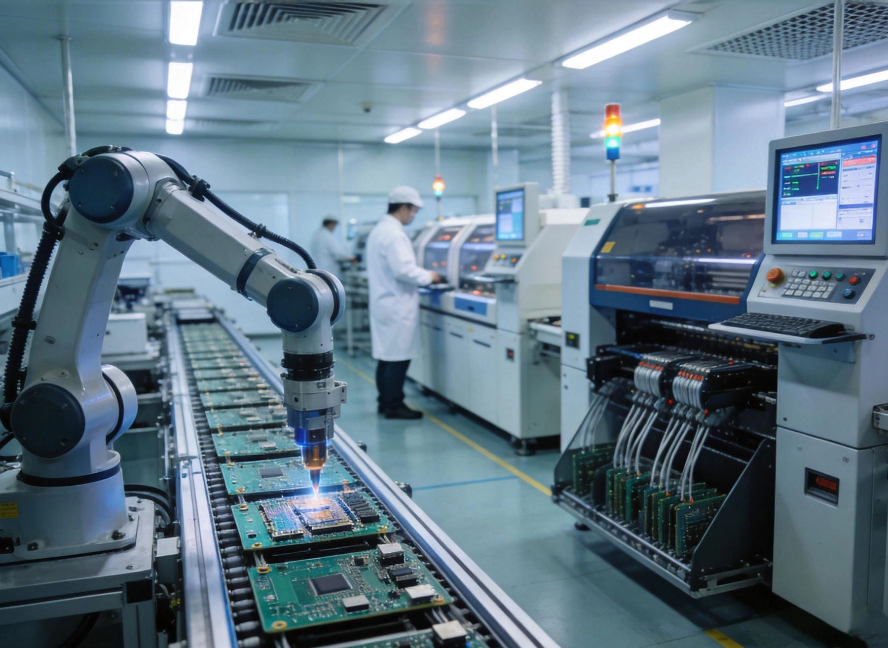
Industrial Pcb Production encompasses the large-scale manufacturing of printed circuit boards designed for commercial, industrial, and professional applications. Unlike hobbyist or prototype PCB Fabrication, industrial production prioritizes consistency, reliability, and cost-effectiveness across thousands or millions of units.
The foundation of any successful PCB production run starts with proper Design For Manufacturing (DFM) review. This critical step ensures that the board design can actually be produced efficiently at scale. Many costly mistakes—both in time and money—can be avoided by catching design issues early in the process.
Understanding each stage of the production process helps appreciate the complexity involved in manufacturing reliable circuit boards. Let's walk through each step in detail.
The journey of an Industrial Pcb begins with selecting the right base material. The substrate—the non-conductive foundation of your board—determines many of its electrical and mechanical properties. For most standard applications, FR-4 (Flame Retardant 4) remains the workhorse material, offering a good balance of cost, performance, and manufacturability.
But industrial applications often demand more specialized materials. High-frequency applications like 5G infrastructure require Rogers or Taconic laminates with controlled dielectric properties. High-power designs might call for metal core substrates like aluminum nitride or IMS (Insulated Metal Substrate) that excel at Heat Dissipation.
Material Selection directly impacts:
For multi-layer PCBs—the kind you'll find in computers, smartphones, and complex industrial equipment—the production process starts with inner layers. This involves several precise steps:
Cleaning and Coating: The copper-clad substrate is thoroughly cleaned to remove any contaminants, then coated with a light-sensitive resist material. Even microscopic particles can cause defects, so cleanroom conditions are essential here.
Exposure and Development: The Pcb Design pattern is transferred onto the board using photolithography. UV light passes through a film of the circuit pattern, hardening the resist where copper traces should remain. The unexposed resist is then washed away.
Copper Etching: The exposed copper is chemically etched away, leaving only the desired circuit pattern. The remaining hardened resist protects these traces. Timing and chemical concentration must be precisely controlled—over-etching thins traces and compromises conductivity, while under-etching creates shorts between adjacent features.
Resist Stripping: The remaining resist is removed, revealing the completed inner layer pattern. Automated optical inspection (Aoi) then checks each panel for defects before proceeding.
For multi-layer boards, getting all layers perfectly aligned is crucial. Misalignment leads to registration errors that can render boards unusable or, worse, cause functional failures in the field.
Industrial facilities use specialized optical alignment systems that can achieve alignment accuracy within 25 microns. During lamination, multiple inner layers are stacked with prepreg (partially cured fiberglass sheets) between them, then pressed together under high heat and pressure. The prepreg melts and flows, bonding all layers into a solid panel.
Common lamination issues include:
Drilling represents one of the most critical and costly operations in PCB production. Holes must be precisely placed to connect different layers electrically. Modern CNC drilling machines can contain over 200 drill heads capable of drilling thousands of holes per minute.
The drilling process involves several hole types:
| Via Type | Purpose | Typical Size |
|---|---|---|
| Through-Hole | Connect all layers | 0.3mm - 6.0mm |
| Blind Via | Connect outer to inner layers | 0.15mm - 0.5mm |
| Buried Via | Connect inner layers only | 0.15mm - 0.5mm |
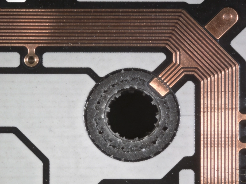
| Microvia | High-density interconnects | 0.05mm - 0.15mm |
After drilling, the holes must be metallized to create electrical connections between layers. This involves a multi-step process of cleaning, micro-etching, and electroless copper deposition followed by electroplating to achieve the required copper thickness.
Once the board is fully interconnected internally, outer layers are processed similarly to inner layers—pattern transfer, exposure, development, and etching. However, outer layers have additional requirements:
Surface Finish Application: Exposed copper must be protected from oxidation while maintaining solderability. Common surface finishes include:
Silkscreen and Legend Printing: Component designators, logos, and other markings are printed onto the board using either inkjet or screen printing. This step ensures assembly technicians can correctly place components during Pcb Assembly.
The final shape of the PCB is cut from the production panel using CNC routing or punching dies. Panelization—the arrangement of individual boards within a larger panel—optimizes material utilization and facilitates handling during assembly.
Common panelization styles include:
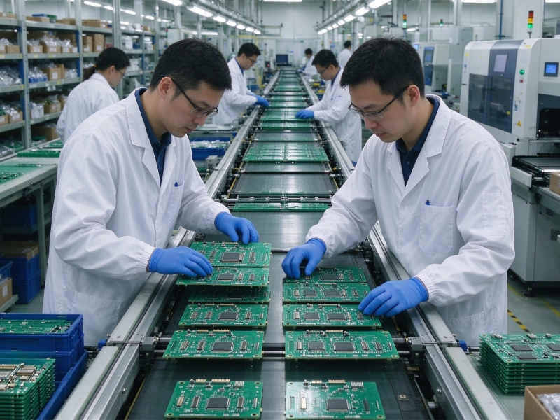
PCB Fabrication creates the bare board, but Pcb Assembly is where components are mounted and the board becomes functional. This process typically follows two main approaches:
While increasingly rare in new designs, through-hole components remain important for applications requiring strong mechanical bonds or high current handling. THT assembly involves:
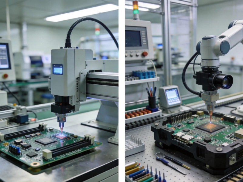
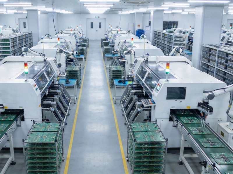
SMT dominates modern Electronics Production, enabling miniaturization and automated mass production. The Smt Assembly line typically includes:
Despite decades of refinement, Industrial Pcb Production faces ongoing challenges that manufacturers must continuously address. Understanding these challenges helps stakeholders make informed decisions about their PCB sourcing and design.
Consumer electronics continue shrinking while adding functionality. This drives demand for finer trace widths, smaller vias, and higher component densities. While 0.4mm pitch BGAs were cutting-edge five years ago, today's flagship smartphones use 0.3mm and even 0.25mm pitch packages. Manufacturers must constantly invest in new equipment and processes to keep pace.
Real-world impact: A minor misalignment that would be acceptable on a 10-year-old product with 0.8mm pitch components becomes a catastrophic defect on modern designs with 0.35mm pitch components.
Power densities in modern electronics continue increasing, particularly in applications like electric vehicles, data centers, and LED lighting. Traditional FR-4 materials have a Glass Transition Temperature (Tg) around 130-140°C, which may be inadequate for high-power applications.
Solutions being implemented: High-tg Materials, metal core substrates, heavy copper designs, Thermal Vias, and integrated heatsink solutions.
With 5G, high-speed data interfaces (USB4, PCIe 5.0, DDR5), and advanced automotive radar systems, Pcb Materials and designs must support increasingly demanding signal frequencies—sometimes exceeding 30GHz.
Key considerations: Controlled Impedance routing, low-loss materials, proper via design, and careful ground plane placement all become critical for reliable performance.
Detecting defects becomes exponentially harder as feature sizes shrink. A missing 10-micron particle that would have been irrelevant 20 years ago can now cause opens or shorts on modern high-density designs.
Modern QA approaches: Automated Optical Inspection (AOI), X-ray Inspection for hidden joints, In-Circuit Testing (Ict), Flying Probe Testing, and Functional Circuit Testing.
Pcb Manufacturing operates on thin margins, yet must continuously invest in expensive new equipment. Raw material costs fluctuate based on copper prices, fiberglass availability, and specialty material demands. The 2020-2023 period demonstrated how quickly supply chain disruptions can impact lead times and pricing.
Industry responses: Diversified supplier relationships, strategic inventory management, and increased automation to reduce labor costs.
Environmental regulations continue tightening globally. RoHS (Restriction of Hazardous Substances) compliance is now baseline, with REACH, California Proposition 65, and emerging regulations around PFAS and plastics adding complexity.
Manufacturing implications: Careful supplier qualification, incoming material testing, documentation tracking, and periodic audits of the entire supply chain.
Professional PCB manufacturers adhere to recognized industry standards that define acceptable quality levels and test methodologies. Understanding these standards helps you specify requirements appropriately for your application.
The Association Connecting Electronics Industries (IPC) publishes the most widely recognized standards for Pcb Manufacturing. Key standards include:
IPC defines three acceptance classes based on product service environment:
Always specify the appropriate class—over-specifying increases cost unnecessarily, while under-specifying risks field failures.
Choosing a manufacturing partner significantly impacts your product's quality, cost, and time-to-market. Consider these factors when evaluating potential suppliers:
The PCB industry continues evolving with new technologies and market demands:
While still nascent, additive PCB manufacturing (printing conductive traces instead of etching) promises faster prototyping, reduced waste, and potential for truly custom geometries.
Embedding passive and active components within the PCB layers rather than on the surface enables further miniaturization and improved electrical performance.
Technologies like chiplets, 2.5D interposers, and embedded die substrates are pushing traditional PCB manufacturing into new territory, blurring lines between semiconductor packaging and PCB production.
From solvent recovery programs to water recycling and renewable energy adoption, environmentally conscious manufacturing is becoming a competitive differentiator.
Whether you're developing a new product or optimizing an existing design, understanding the Industrial Pcb production process empowers better decision-making. Consider reaching out to multiple manufacturers for quotes, and always request DFM feedback early in your design cycle.
Standard lead times range from 5-15 business days for production quantities, depending on board complexity, layer count, and manufacturer capacity. Expedited services typically add 30-50% cost for 48-72 hour turns.
Costs vary dramatically based on specifications—a simple 2-layer board might cost $5-20 per unit in high volumes, while complex 12-layer HDI boards for smartphones can exceed $200 per unit. Always request quotes for your specific design.
Many manufacturers now offer low-MOQ programs starting at 5-10 units for prototyping, while traditional production MOQs often start at 100-500 units. Some manufacturers offer a hybrid model with moderate setup fees enabling small-to-medium runs.
Submit your design files (Gerber, NC drill, BOM) to your manufacturer for a Dfm Review before releasing for production. Most reputable manufacturers provide this service free or for a nominal fee, potentially saving thousands in retooling costs.
Standard testing typically includes AOI for visual defects and flying probe or fixture-based electrical testing. Additional services like X-ray Inspection, microsection analysis, and Functional Testing may be available for critical applications.
Industrial PCB production represents a remarkable feat of modern engineering—transforming raw materials into the sophisticated platforms that power our connected world. From carefully selecting substrate materials through dozens of precision manufacturing steps, every board that rolls off a production line embodies decades of accumulated industry knowledge.
Understanding this process equips you to make better design decisions, communicate more effectively with manufacturers, and troubleshoot issues when they arise. Whether you're an engineer specifying boards for the next breakthrough product, an entrepreneur bringing a new device to market, or simply curious about the technology around you, we hope this guide has illuminated the fascinating world of industrial PCB production.
The challenges are real—miniaturization, Thermal Management, Signal Integrity, cost pressure, and environmental compliance all demand constant attention. Yet the industry continues innovating, pushing boundaries of what's possible in electronic interconnection. As new applications emerge in electric vehicles, IoT devices, and beyond, industrial PCB production will remain fundamental to technological progress.
Understanding the Lifecycle of an Industrial PCB Production RunJuly/31/2026

How Automation is Revolutionizing Industrial PCB Production in 2026September/02/2026
5 Critical Steps to Optimize Your Industrial PCB Production WorkflowJuly/15/2026
Cost Reduction Strategies in High-Volume Industrial PCB ProductionSeptember/18/2026
Navigating Supply Chain Challenges in Global Industrial PCB ProductionOctober/14/2026
Key Differences Between Consumer and Industrial PCB ProductionJune/27/2026
How to Scale Your Industrial PCB Production for Mass ManufacturingJune/02/2026
Identifying and Fixing Micro-Vias Issues in Industrial PCB Quality InspectionsSeptember/10/2026