

Home Blog Industrial PCB DFM & Design
  1. July/03/2026How to Avoid Costly Mistakes with Proper Industrial PCB DFM
    How to Avoid Costly Mistakes with Proper Industrial PCB DFM
  2. June/08/2026Essential Rules for Industrial PCB Design
    Essential Rules for Industrial PCB Design
  3. May/27/2026Essential Rules for Industrial PCB Design
    Essential Rules for Industrial PCB Design

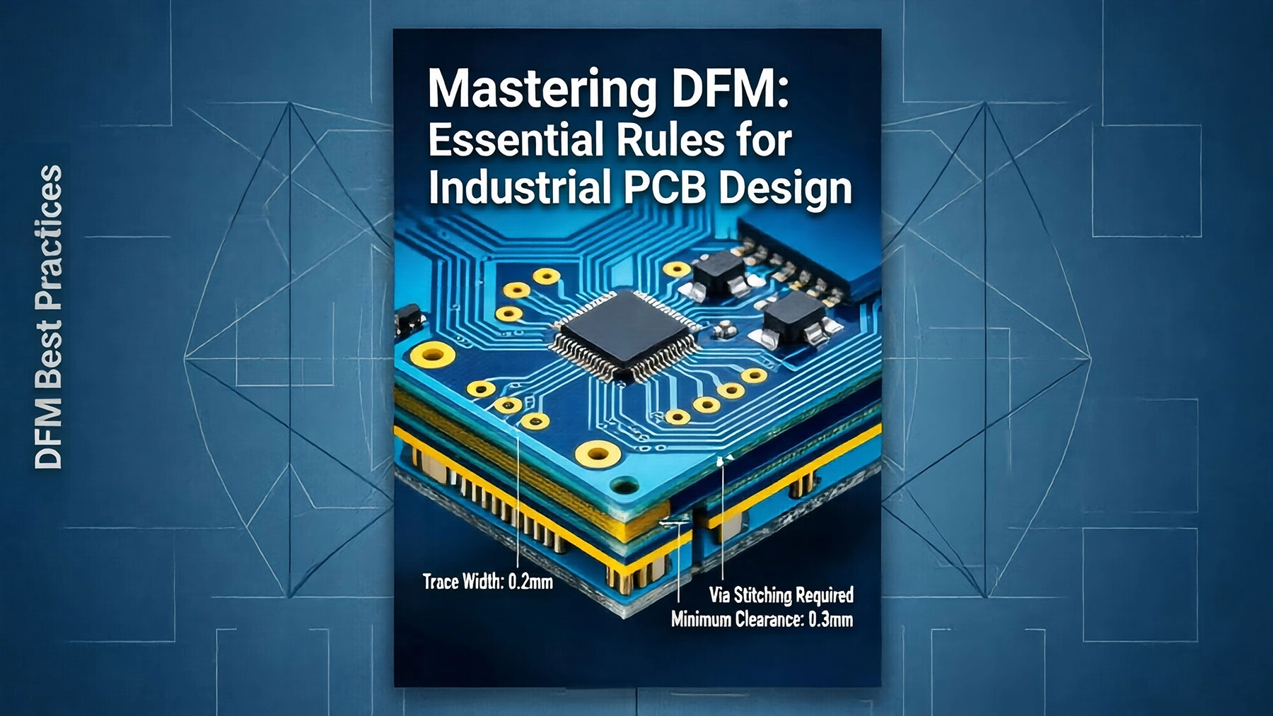
Industrial PCB DFM & Design

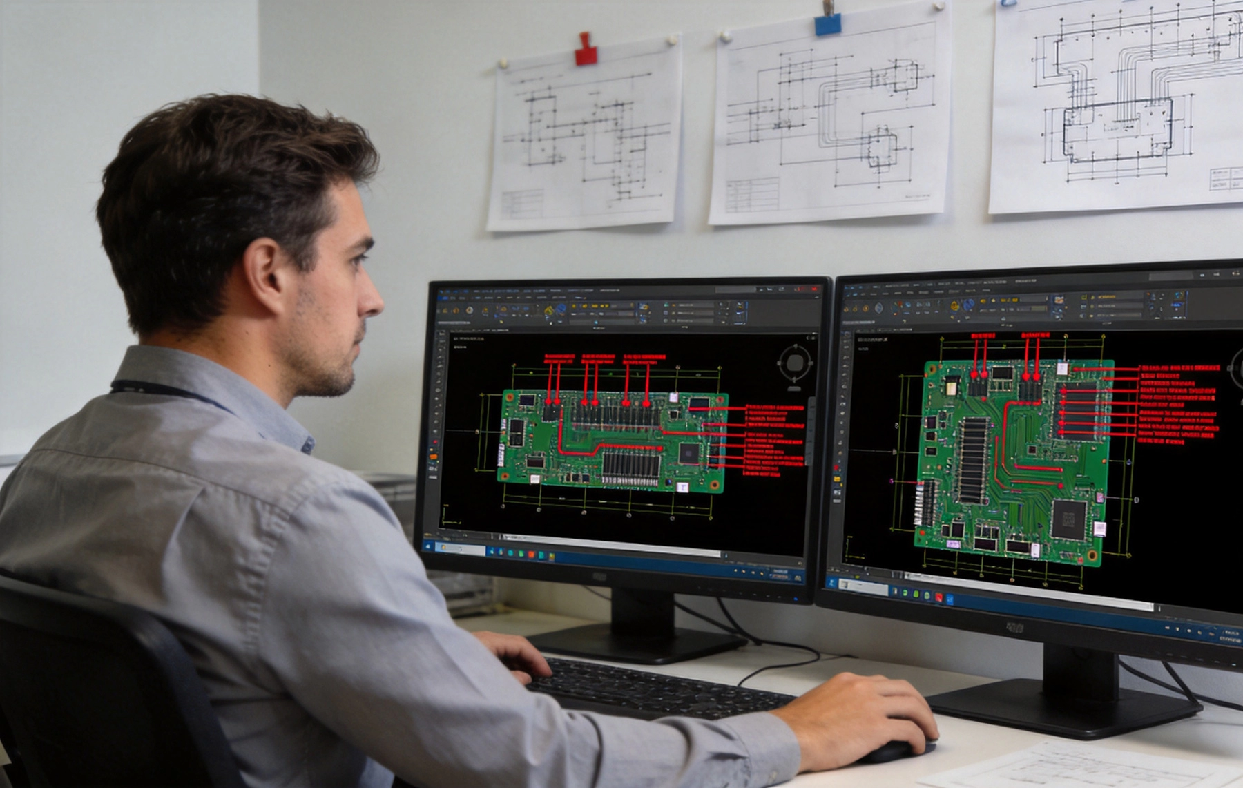
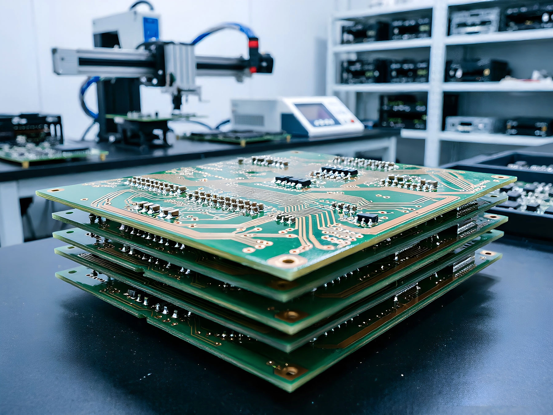
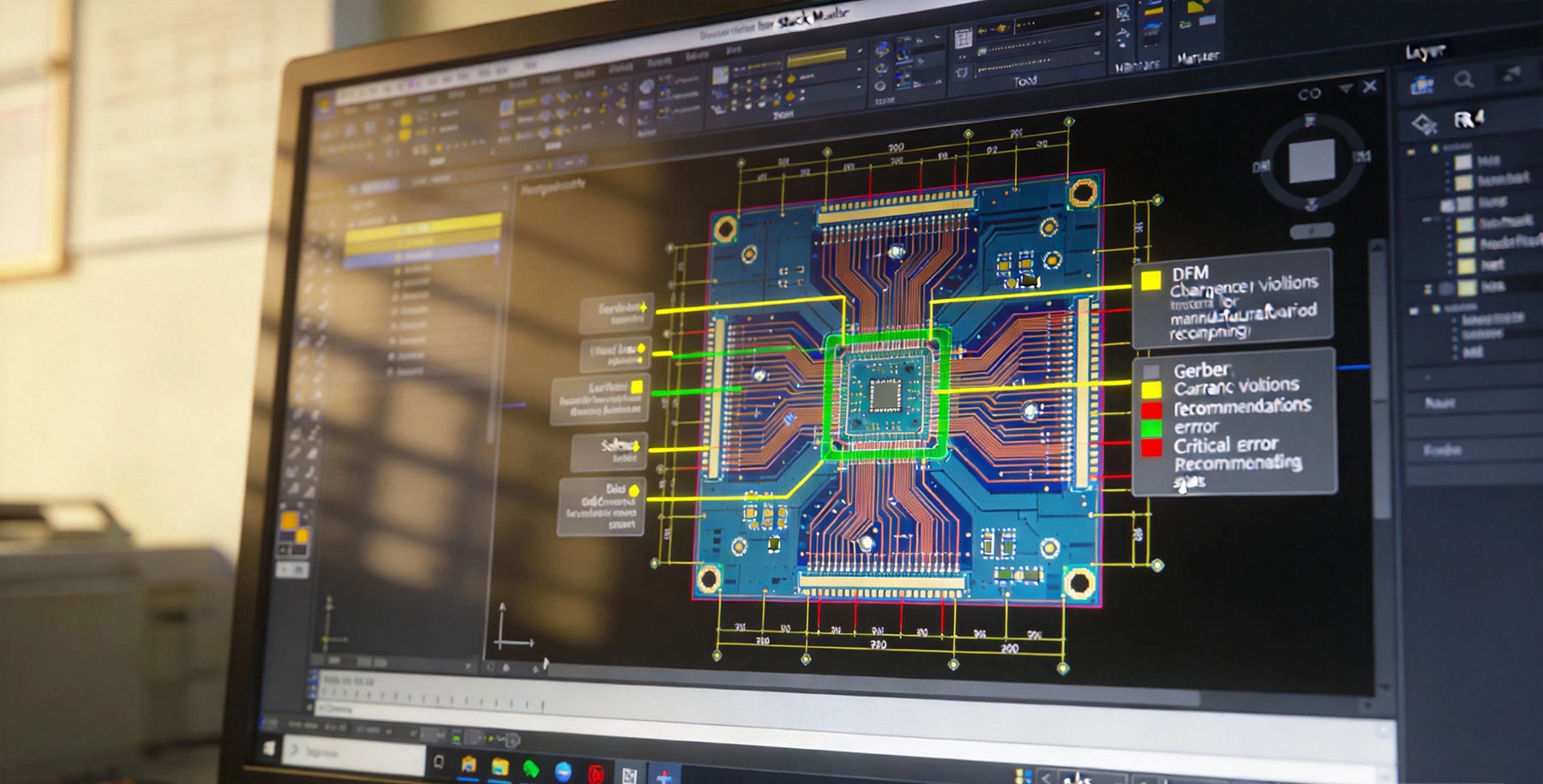
is a critical engineering methodology that bridges the gap between theoretical circuit design and practical Industrial Pcb Manufacturing. By integrating manufacturing constraints early in the design phase, engineers can preemptively eliminate potential production risks and ensure robust performance.

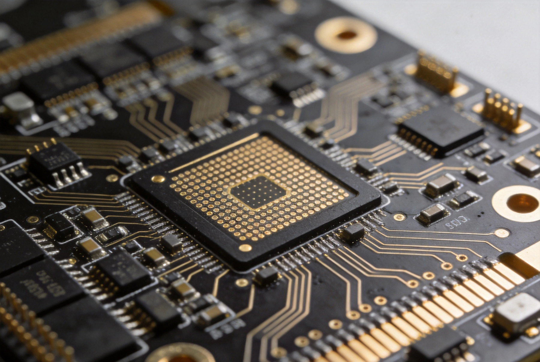
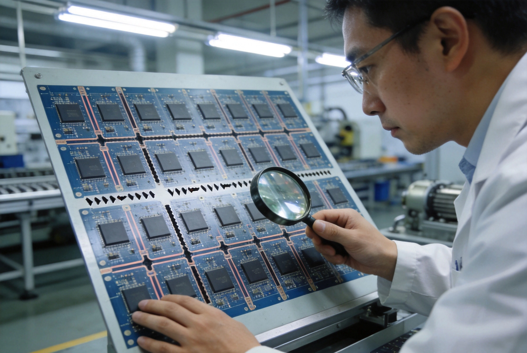
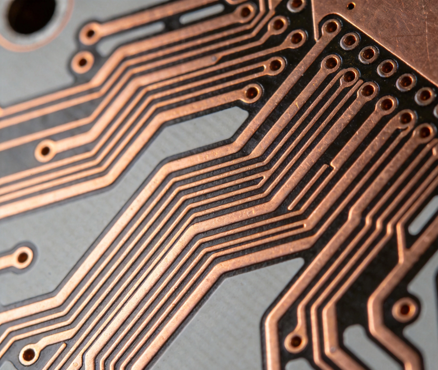
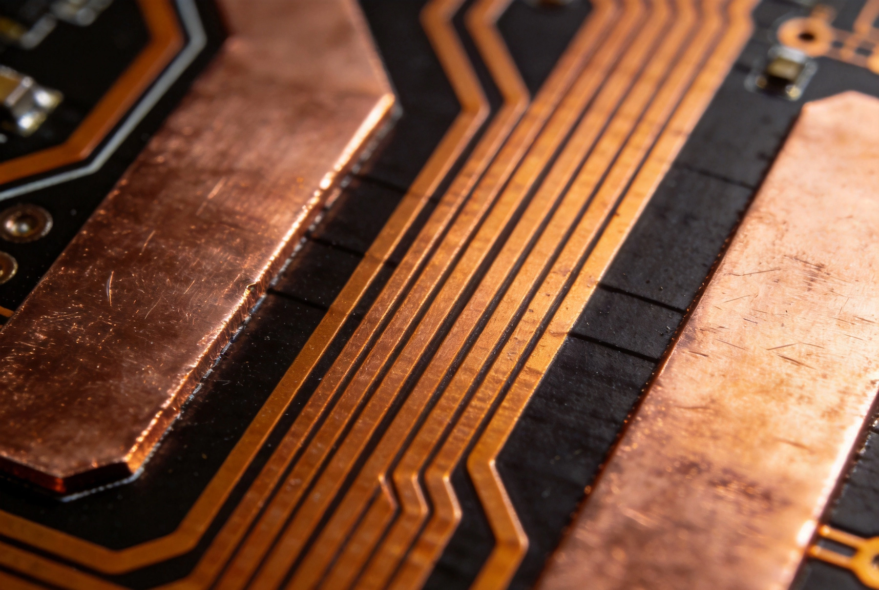
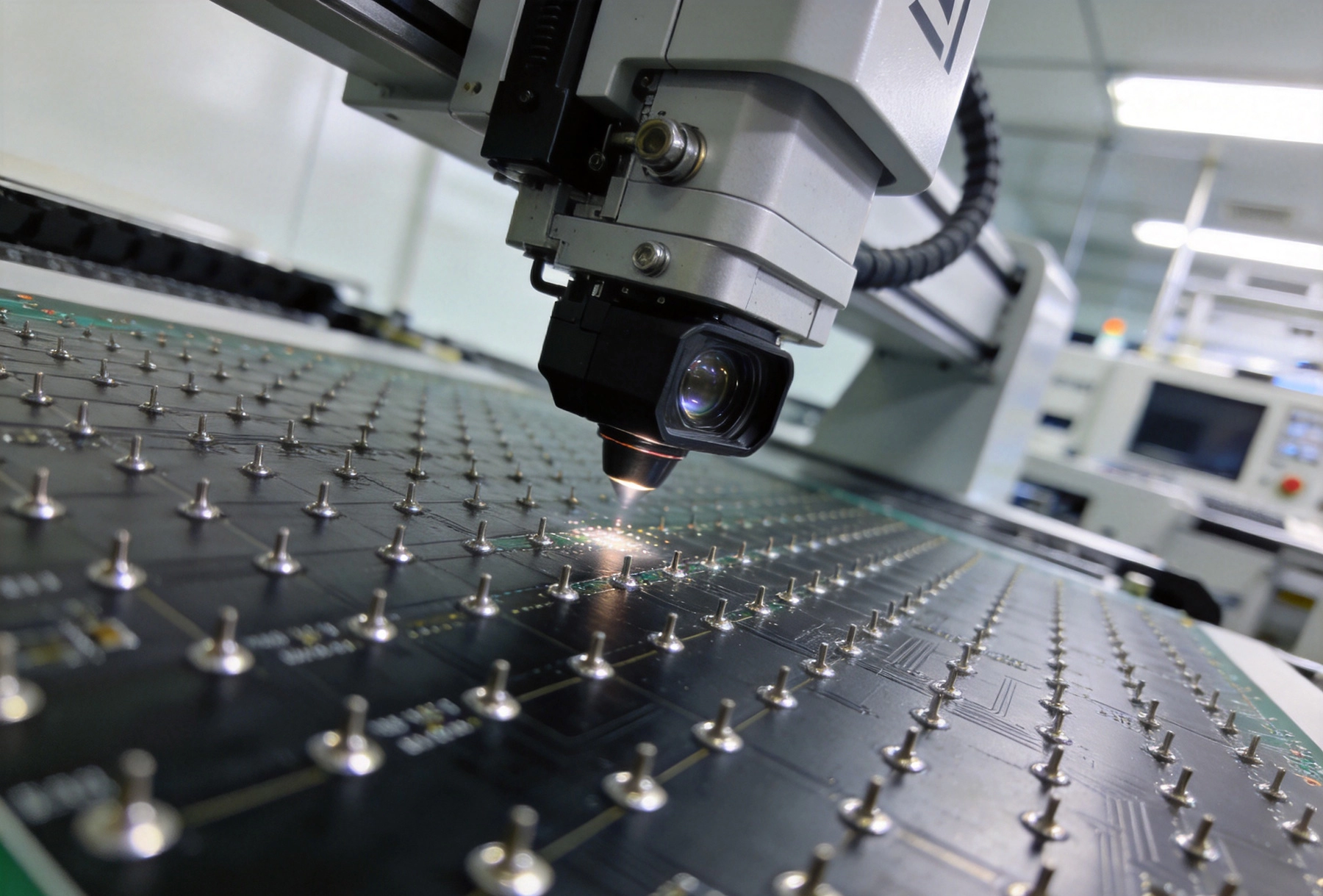
Key DFM strategies include optimizing trace widths and spacing to match the fabrication capabilities for heavy copper layers, ensuring adequate annular rings to withstand mechanical stress, and implementing symmetrical stack-ups to prevent board warping during thermal cycling. Furthermore, proper component placement and the inclusion of fiducial marks facilitate precise automated assembly and rigorous quality inspection. Adhering to strict DFM guidelines significantly reduces fabrication defects, lowers overall production costs, and guarantees the high reliability required for mission-critical Industrial Electronics operating in harsh environments.

Send Message
Name*
E-mail*
Country*
Phone/WhatsApp*
Name*
E-mail*
Country*
Phone/WhatsApp*