Open Nav


You know that sinking feeling when a prototype works perfectly, but the first production run comes back with 30% of the boards failing? It is a nightmare. Industrial environments are brutal, with vibration, heat, and EMI everywhere. Mastering DFM: Essential Rules for Industrial Pcb Design is the only way to ensure your board survives the factory floor and the field. I have spent years fixing boards that were designed without manufacturing in mind, and trust me, it is expensive. Let’s dive into the practical rules that will save your project.
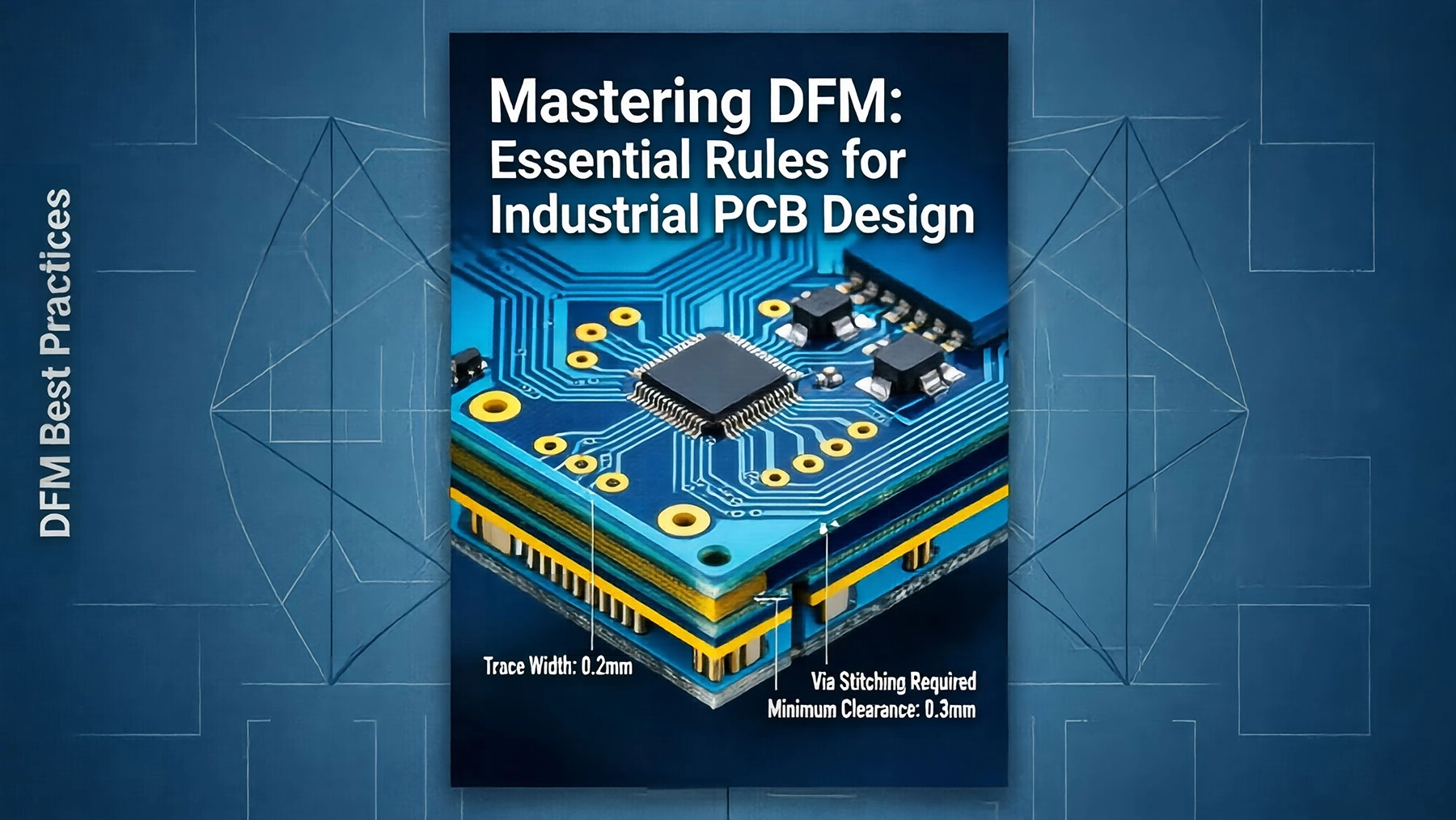
Consumer electronics are designed to last a few years. Industrial PCBs need to run for decades, often in dusty, hot cabinets. When you are mastering DFM: Essential Rules for Industrial Pcb Design, you have to think about the assembly line first. Can a pick-and-place machine actually grab that tiny 0201 resistor next to a massive transformer? Probably not. The shadow effect during reflow soldering will cause cold joints. You need to maintain proper clearance between components. I always recommend at least 0.5mm between small parts and tall ones, but for industrial vibration, even more is better.
Also, consider the testing phase. If you don't leave test points, how will you troubleshoot a board inside a sealed metal enclosure? Mastering DFM: Essential Rules for Industrial Pcb Design means adding dedicated test pads for critical nets. Don't rely on probing tiny vias. Make it easy for the test engineer, and they will make your life easier.
Trace width is not just about current carrying capacity; it is about manufacturability. Etching is a chemical process, and it is not perfect. If you design a 4-mil trace, the factory might etch it down to 3 mils, causing an open circuit under high current. When mastering DFM: Essential Rules for Industrial Pcb Design, stick to standard capabilities. I usually keep signal traces at 6 mils or wider, and power traces much larger. A good rule of thumb is 1mm of width per amp of current, but check the IPC-2221 standards.
Avoid sharp 90-degree corners. While the old myth about RF radiation is mostly exaggerated for industrial control boards, acute angles can trap acid during etching, leading to under-etching. Use 45-degree angles or curved traces. It is a small change that improves yield significantly.
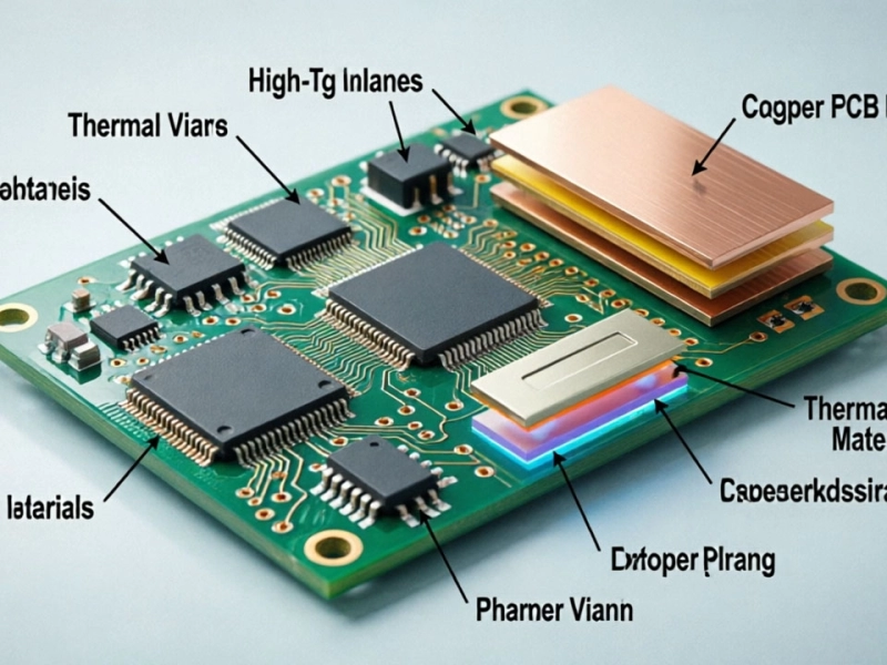
Vias are weak points in industrial boards. If you place a via directly in a pad without plugging it, solder will wick down into the hole during wave soldering. This leads to dry joints. When mastering DFM: Essential Rules for Industrial Pcb Design, use tented vias or specify Via-in-pad with resin fill for BGA escapes. For power components, Thermal Vias are essential. But don't just drill a hundred holes randomly. Array them properly under the thermal pad to ensure even heat transfer to the inner copper planes.
Speaking of heat, don't put all your hot components in one corner. This creates a thermal hotspot that can warp the board during reflow. Spread them out. And remember, industrial boards often use Conformal Coating. Make sure your connectors and switches are masked or positioned so the coating doesn't interfere with their function.
A messy silkscreen is a sign of a messy design. If the technician cannot read the polarity marking for a capacitor, they will guess. And they will guess wrong. Mastering DFM: Essential Rules for Industrial Pcb Design includes clear, readable silkscreen. Keep text away from pads and vias. Use a font size that is at least 40 mils high if possible. Also, add a Pin 1 indicator for every IC. A simple triangle or dot saves hours of debugging.
Don't forget fiducials. Global fiducials are good, but local fiducials for fine-pitch components are better. They help the vision system align the nozzle precisely. In an industrial setting where reliability is key, these little copper dots are your insurance policy.
Designing for manufacturing is not about limiting your creativity; it is about making your creativity realizable. When you focus on mastering DFM: Essential Rules for Industrial PCB Design, you are building a product that respects the realities of physics and factory economics. It takes a bit more time upfront, but it prevents the costly spin cycles that kill project budgets.
Take a look at your current layout. Are your components aligned? Are your test points accessible? Is your silkscreen legible? Fix these things now, before you hit the "Generate Gerbers" button. Your future self, and your production manager, will thank you.
Q: What is the minimum trace width for industrial PCBs?
A: While some fabs can do 3-4 mils, for industrial reliability and etching consistency, I recommend staying above 6 mils for signals and sizing power traces based on IPC-2221 current tables plus a safety margin.
Q: Do I really need test points on every net?
A: Not every net, but definitely all critical signals, power rails, and communication buses. In industrial maintenance, being able to hook up an oscilloscope without desoldering components is invaluable.
Q: How do I prevent solder wicking in vias?
A: Use tented vias (covered by solder mask) for non-plugged holes. For BGAs or high-reliability areas, specify resin-filled and copper-capped vias.
Essential Rules for Industrial PCB DesignMay/27/2026
Optimizing Trace Width and Spacing in Industrial PCB DFMAugust/06/2026

Design for Testability (DFT): A Crucial Aspect of Industrial PCB DesignJuly/20/2026
Design Rules for Heavy Copper Traces in Power ElectronicsJuly/27/2026
How to Avoid Costly Mistakes with Proper Industrial PCB DFMJuly/03/2026

Understanding CTE and Its Impact on Industrial PCB Materials SelectionJuly/18/2026
Thermal Management Strategies for Long-Term Industrial PCB ReliabilityJune/04/2026
Why Choose Rigid-Flex PCB Solutions for Complex Industrial Assemblies?June/17/2026