Open Nav


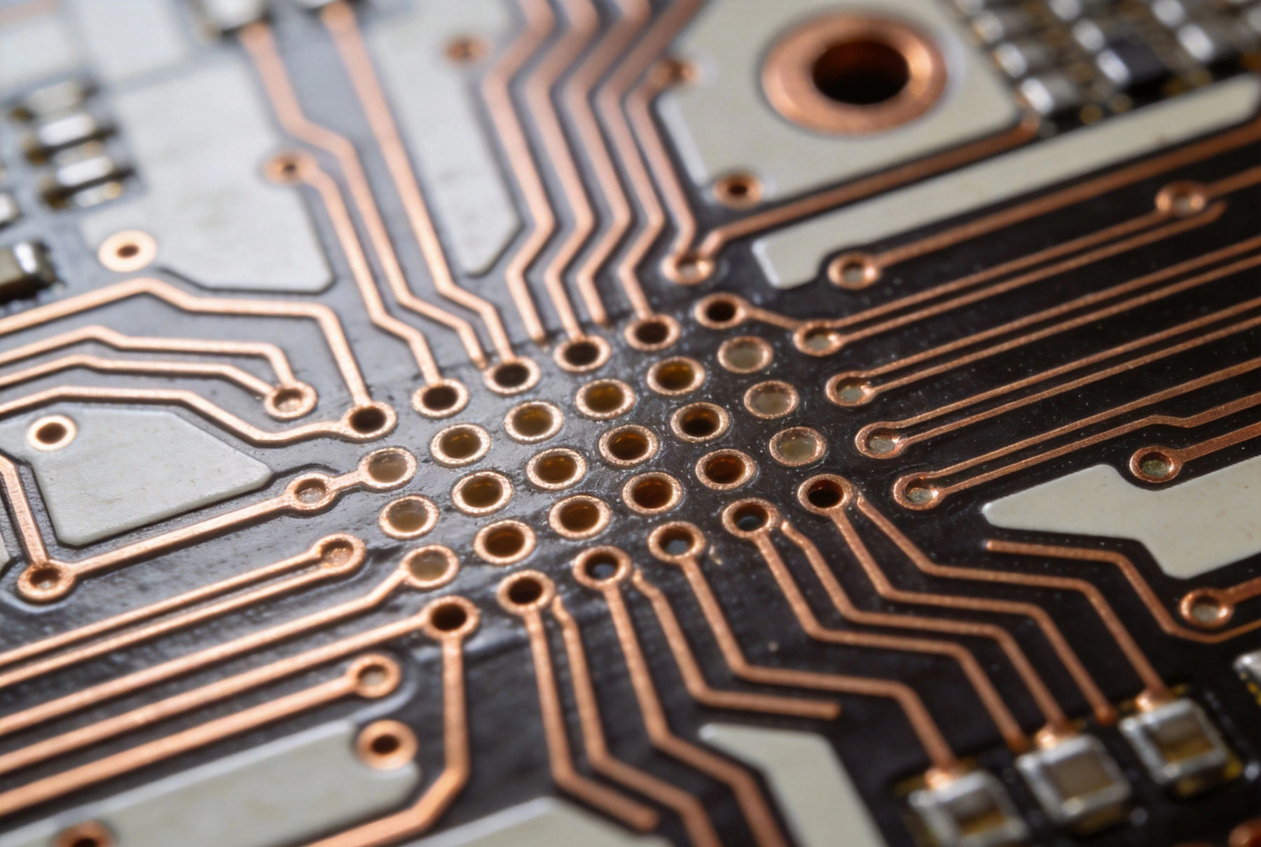
Walk through any modern industrial facility, and you'll notice something remarkable: the electronic systems controlling machines, sensors, and processes are getting smaller and more sophisticated. Factory floor controllers that once required cabinet-sized enclosures now fit in handheld devices. Sensor modules packed with processing power wirelessly transmit data from remote locations. Industrial IoT deployments place sophisticated electronics in equipment that was previously purely mechanical.
This transformation toward compact Industrial Electronics is driven by multiple factors: the need for distributed intelligence in industrial IoT, space constraints in machinery and equipment, demands for portability and modularity, and relentless pressure to reduce costs through miniaturization. Behind this evolution lies a critical enabler: HDI (High Density Interconnect) PCB technology.
HDI PCBs have revolutionized how Industrial Electronics are designed and manufactured, enabling unprecedented functionality in incredibly compact packages. Understanding Hdi Technology has become essential for industrial electronics engineers, designers, and product developers who need to push performance boundaries while shrinking form factors.
In this comprehensive introduction, we'll explore what Hdi Technology is, how it works, why it matters for industrial applications, and how you can leverage it in your next industrial electronics project.
HDI stands for High Density Interconnect, referring to advanced PCB technology that achieves significantly higher wiring density than conventional PCBs through smaller features and specialized structures. HDI PCBs are characterized by:
These features collectively enable HDI PCBs to achieve 2-3x the wiring density of conventional PCBs with the same footprint, supporting more components, higher performance, and greater functionality in smaller packages.
PCB technology has evolved through distinct generations:
HDI represents the current frontier of PCB technology, pushing boundaries of what's possible in circuit board design. While originally developed for consumer electronics like smartphones, HDI technology has matured and become cost-effective for industrial applications where its capabilities provide substantial advantages.
Microvias are the defining feature of HDI technology. Unlike mechanically drilled through-holes that penetrate the entire board thickness, microvias are laser-drilled and typically only go through a few layers:
Microvias consume far less space than through-holes and enable more efficient routing. A 100μm microvia occupies roughly 1/100th the area of a 1mm through-hole, dramatically increasing available routing area.
HDI boards are constructed using build-up processes:
This build-up approach enables HDI boards with 8, 12, 16, or more layers while maintaining overall thickness comparable to conventional 4-6 layer boards. More layers mean more routing channels and better Signal Integrity without increasing board thickness.
Advanced HDI boards employ sophisticated via arrangements:
These arrangements maximize space efficiency while maintaining electrical characteristics. Complex HDI boards might have thousands of microvias in intricate patterns enabling dense routing.
HDI technology uses specialized materials:
Thinner materials enable more layers in the same overall thickness, which is critical for industrial applications where board thickness is constrained by mechanical packaging requirements.
Industrial electronics often face severe space constraints:
HDI technology enables these applications by packing more functionality into smaller spaces. What would have required separate PCBs or larger form factors becomes possible with HDI's increased density.
The rise of Industrial IoT creates specific needs that HDI addresses:
These capabilities together require significant circuit complexity. HDI makes it possible to integrate all these functions into compact sensor nodes and edge computing modules that fit within equipment or enclosures.
Beyond size, HDI offers performance advantages for industrial electronics:
For high-speed digital interfaces, precision analog sensing, or RF applications critical in industrial settings, HDI's improved electrical characteristics directly enhance performance.
Industrial electronics face harsh conditions:
HDI technology, when properly designed and manufactured, provides reliability comparable to conventional PCBs. Microvias, when correctly plated, provide robust interconnections. The key is working with manufacturers experienced in industrial HDI applications who understand the reliability requirements.
The simplest HDI configuration:
This configuration provides modest density improvements at reasonable cost, suitable for applications where space savings are important but not critical.
More advanced HDI:
This configuration represents the sweet spot for many industrial applications—substantial density improvements without the complexity and cost of the most advanced HDI structures.
The most advanced HDI configuration:
This configuration provides the ultimate in density but is overkill for many industrial applications. Reserved for the most space-constrained, highest-performance designs where cost is secondary to capability.
Industrial applications typically benefit from 2+N+2 structures:
More complex structures make sense only for applications where the additional density directly enables product features that would otherwise be impossible.
HDI boards require careful DFM attention:
Working with your PCB manufacturer early in design prevents costly iterations. The best HDI manufacturers provide DFM feedback that catches issues before prototyping.
HDI boards enable better signal integrity but require proper design:
For industrial systems with high-speed interfaces (Ethernet, USB, CAN, etc.), HDI's tighter tolerances improve signal quality, but you must design properly to realize these benefits.
More components in smaller spaces create thermal challenges:
Industrial applications often operate in high-temperature environments. Proper thermal design ensures reliability under these conditions.
HDI boards enable advanced components:
Select components compatible with HDI assembly processes. Ensure your manufacturer can handle the packages you plan to use.
Microvias are created with precision lasers:
Laser Drilling capability is the gateway to HDI technology. Not all PCB manufacturers have laser drilling equipment, which affects their HDI capabilities.
Build-up layers are added sequentially:
Each lamination cycle adds complexity and cost but enables the layer stacking that makes HDI possible.
Reliable microvia plating is critical:
Improper microvia plating leads to reliability issues. Experienced manufacturers have proven processes and Quality Control for microvia plating.
HDI boards cost more than conventional PCBs due to:
However, HDI costs have decreased significantly as the technology has matured. For many industrial applications, the benefits outweigh the additional cost.
When evaluating HDI costs, consider:
Often, the total product cost with HDI is lower than with conventional PCBs when you account for mechanical packaging savings and performance benefits.
Reduce HDI costs through:
Smart design choices can significantly impact HDI costs without compromising functionality.
Compact sensor nodes with multiple sensing capabilities:
HDI enables all these functions in sensor modules that fit inside equipment or remote locations.
Compact controllers for machinery and processes:
HDI controllers fit in tight spaces within equipment while maintaining full functionality.
Local intelligence for Industrial IoT:
HDI enables sophisticated edge computing in compact form factors suitable for distributed deployment.
Handheld and portable industrial tools:
HDI's density advantages directly enable smaller, lighter portable equipment.
Evaluate manufacturers on:
Not all HDI manufacturers have equal capabilities. Verify their actual experience with industrial HDI boards.
Assess quality systems:
HDI reliability directly impacts product reliability. Partner with manufacturers who prioritize quality over speed.
Strong partnerships require:
The best HDI partners become extensions of your engineering team, providing expertise throughout development.
Continuous Improvement in capability:
These advances will enable even greater density for future industrial electronics.
New materials expanding capabilities:
Material advances will expand HDI applicability to new industrial use cases.
Convergence with semiconductor packaging:
These integrations will blur the lines between PCB and semiconductor packaging, creating new possibilities.
HDI technology has matured from consumer electronics to become a practical, powerful enabler for compact industrial electronics. The ability to pack more functionality into smaller spaces is transforming industrial systems, enabling new product categories, and supporting the rise of Industrial IoT and edge computing.
For industrial electronics engineers and product developers, understanding HDI technology is no longer optional—it's essential for staying competitive in markets that demand smaller, smarter, more capable products. The right HDI implementation reduces product size, improves performance, and creates competitive advantages.
Success with HDI requires partnering with capable manufacturers, designing for manufacturability, and understanding the trade-offs between density, cost, and reliability. When implemented properly, HDI enables industrial products that would be impossible with conventional PCB technology.
The industrial electronics landscape continues evolving toward greater intelligence, connectivity, and miniaturization. HDI technology provides the foundation for this evolution. Whether you're developing sensor nodes, compact controllers, or edge computing systems, HDI deserves serious consideration as a key enabling technology.
The compact industrial electronics of today and tomorrow will rely on HDI technology. Understanding and leveraging this technology positions you to design innovative products that meet the demanding requirements of modern industrial applications.
HDI PCBs use microvias (laser-drilled holes under 150μm), finer traces and spaces (30-50μm vs 100-150μm), thinner dielectrics, and blind/buried vias to achieve 2-3x the wiring density of standard PCBs. This enables more components and functionality in the same space or equivalent functionality in smaller space.
Consider HDI when your industrial application has severe space constraints, requires multiple wireless modules, needs high component density for sensor fusion or edge computing, or when conventional PCBs can't fit within mechanical packaging. If board space is limiting your design, HDI is likely worth considering.
Yes, when properly designed and manufactured by experienced partners, HDI PCBs provide reliability comparable to conventional PCBs. Key factors include proper microvia plating, appropriate Material Selection for industrial temperatures, and working with manufacturers who understand industrial reliability requirements.
HDI PCBs typically cost 50-150% more than conventional PCBs depending on complexity (1+N+1, 2+N+2, or any-layer structures) and volume. However, total product cost often decreases when accounting for smaller enclosures, reduced assembly costs, and performance benefits. Cost depends heavily on layer count and microvia density.
2+N+2 structures typically offer the best balance for industrial applications—significant density improvements at reasonable cost with proven manufacturability and reliability. More complex any-layer HDI structures are usually overkill unless extreme density is absolutely required.
Most components work on HDI boards, but HDI enables use of fine-pitch packages (BGAs, QFNs) with pitches under 0.5mm that conventional boards struggle with. Verify your manufacturer can assemble the specific components you plan to use, especially fine-pitch BGAs and CSPs.
Work closely with your PCB manufacturer early in design. Follow their DFM guidelines for microvia spacing, trace and space, pad sizes, and layer stack-up. Request Dfm Review before prototyping to catch manufacturability issues. The best manufacturers provide specific feedback tailored to your design.
HDI boards require comprehensive testing including electrical testing (flying probe or Ict), Aoi inspection, X-ray Inspection for BGAs and microvias, and cross-sectional analysis to verify microvia plating quality. Functional Testing verifies complete operation per your specifications.
Design Guidelines for Durable Flex PCB Solutions in Dynamic ApplicationsJuly/10/2026
Thermal Resistance and Dielectric Layers in Metal Core PCB SolutionsOctober/12/2026
Unlocking Performance with High-Layer Count Industrial PCB SolutionsJune/15/2026
Stack-up Design Strategies for High-Layer Count Industrial PCBsOctober/09/2026
Material Selection Guide for High-Speed Industrial PCB SolutionsJuly/14/2026
Via-in-Pad and Microvias: Key Features of Advanced HDI SolutionsJuly/26/2026

How to Find the Right Partner for Your Custom Industrial PCB SolutionsJuly/24/2026
Innovative Industrial PCB Solutions for Renewable Energy SystemsAugust/10/2026