Open Nav


When your application demands currents that exceed what standard PCB copper can handle, you face a fundamental design challenge. Standard copper weight of one or two ounces works fine for signal routing and low-Power Distribution, but industrial Power Electronics, motor drives, welding equipment, and renewable energy systems routinely require current capacity that standard PCBs simply cannot provide. Heavy copper PCBs offer the solution— Thick Copper conductors that handle tens or hundreds of amps while maintaining the compact packaging and Manufacturing Efficiency that PCB technology provides.
Chinese manufacturers have developed substantial Heavy Copper Pcb capabilities to serve the global Industrial Electronics market. Facilities across Guangdong, Jiangsu, and other manufacturing provinces now produce heavy copper boards meeting rigorous quality standards for demanding applications. Understanding Heavy Copper Pcb technology, its capabilities, its limitations, and its manufacturing considerations prepares you to specify and source these boards effectively.
This guide covers everything engineers and procurement professionals need to know about heavy copper PCBs for industrial applications. From fundamental design principles to manufacturing considerations in China, we explore the technical and commercial aspects that determine project success.
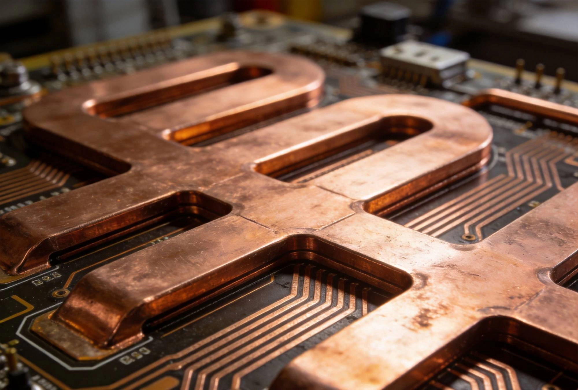
Standard PCB copper weights range from half ounce to two ounce per square foot. Heavy copper boards typically start at three ounces and commonly reach five, ten, or even twenty ounces. Some specialized manufacturers can produce boards with copper exceeding 400 ounces— essentially solid copper structures with circuit features machined into them. The defining characteristic isn't a specific copper weight but rather copper thickness significantly exceeding standard PCB production.
Heavy copper serves applications requiring high current-carrying capacity, low impedance Power Distribution, or both. Electric vehicle charging infrastructure uses heavy copper for its high current requirements. Industrial motor drives need heavy copper to handle the substantial currents flowing through power stages. Solar inverters and wind turbine converters employ heavy copper to manage the power levels these systems handle. Each application has specific current, thermal, and mechanical requirements that drive Copper Weight Selection.
The transition from standard to heavy copper affects almost every aspect of Pcb Design and manufacturing. Trace widths increase dramatically— a 20 amp trace at two ounce copper might be two inches wide, while the same current at four ounce copper requires only one inch. This reduction in trace width enables more compact designs, but it requires changes to artwork, imaging, and plating processes that add manufacturing complexity and cost.
Heavy copper's electrical benefits extend well beyond simple current capacity. The lower resistance of Thick Copper reduces voltage drop along power distribution paths. In high-current systems, voltage drop in PCB traces can represent significant losses— a 0.5 volt drop at 100 amps wastes 50 watts of power and generates unwanted heat. Heavy copper traces minimize these losses, improving system efficiency and reducing Thermal Management burden.
Inductance in power distribution networks affects switching performance in Power Electronics. Heavy copper's larger cross-sectional area reduces loop inductance, improving the performance of synchronous buck converters, motor drive bridges, and other high-speed power switching circuits. This inductance reduction becomes increasingly important as switching frequencies increase in modern power electronics designs seeking smaller magnetic components.
The thermal performance improvements from heavy copper support higher power densities. Heat generated in copper traces spreads more effectively in thick copper, reducing localized hot spots. Combined with Thermal Vias connecting surface traces to internal planes, heavy copper construction creates effective heat spreading paths that move thermal energy away from heat-generating components. This Thermal Management capability often drives heavy copper selection even when current capacity alone wouldn't require it.
Heat Dissipation represents the central challenge in high-current Pcb Design. Heavy copper helps manage heat, but thoughtful thermal management remains essential. The heat generated in traces and components must flow somewhere— either into the PCB material, into attached heat sinks, or into forced air or liquid cooling systems. Heavy copper's Thermal Conductivity (approximately 400 W/mK versus FR-4's 0.3 W/mK) makes it an excellent heat spreading medium.
Thermal Via arrays connect heavy copper surface traces to internal ground and power planes, creating effective heat sinking structures. These Thermal Vias should be placed strategically under components and along high-current traces. Via placement density affects Thermal Resistance— more vias closer together provide lower Thermal Resistance to internal planes. Standard Thermal Via practice works, but heavy copper designs often benefit from more aggressive thermal via patterns due to the higher heat fluxes involved.
FR-4 substrate thermal limits constrain ultimate power handling. Even with excellent copper thermal spreading, the PCB dielectric material limits how much heat can flow into internal planes. For extreme power levels, alternative substrates like aluminum-backed boards or ceramic substrates may be required. However, for most industrial applications in the tens to hundreds of amps range, FR-4 heavy copper construction handles thermal requirements adequately when properly designed.
Chinese PCB manufacturers have invested significantly in heavy copper capabilities to serve Industrial Electronics customers globally. The equipment required for heavy copper production— thicker copper coils, specialized plating tanks, improved imaging systems— represents substantial capital investment that major Chinese manufacturers have made. Most can produce heavy copper boards from three ounce through ten ounce copper with standard turnaround times.
Extremely heavy copper weights may require specialized facilities. Boards exceeding ten ounce copper often need longer processing times and potentially different manufacturing approaches. Some Chinese manufacturers specialize in ultra-heavy copper boards for applications like welding equipment and large-format power distribution. Verify your target manufacturer's specific capabilities for the copper weight your design requires.
Quality systems at major Chinese heavy copper facilities typically include statistical process control for plating thickness, XRF measurement verification of copper weight, and electrical testing of finished boards. These capabilities provide confidence that the copper weight you specify is what you receive. Request documentation of these quality processes when evaluating manufacturers— reputable suppliers gladly share this information.
Heavy Copper Pcb design requires adjusted design rules compared to standard boards. Minimum trace widths increase because the etching process must remove more copper to create the same geometry. Standard Pcb Design Rules specifying five mil traces don't apply when you're working with four ounce or six ounce copper— minimum trace widths may increase to twenty mils or more depending on the copper weight and manufacturer capabilities.
Annular ring requirements for through holes also change with heavy copper. The Plating Process for heavy copper boards must fill holes adequately while maintaining consistent thickness on barrel walls. Standard annular ring specifications may not provide sufficient copper around holes for reliable plating. Consult your manufacturer's design rules for specific annular ring minimums for your target copper weight.
Routing and panelization considerations affect heavy copper designs. Thick copper creates substantial mechanical stress during manufacturing. Internal routed slots and cutouts may require additional support structures or different routing approaches to prevent panel breakage. Your Chinese manufacturer can advise on specific panelization and routing requirements for your board size and copper weight.
One of heavy Copper Pcb's practical advantages: you can mount standard surface mount components on heavy copper boards. This capability enables hybrid designs where heavy copper handles power distribution while standard components handle control and signal functions. The thermal management benefits of heavy copper actually help keep mounted components cooler, improving reliability.
Component attachment to heavy copper requires attention to thermal aspects. Soldering heavy copper planes conducts heat away from solder joints rapidly during assembly. Your assembly process may need temperature profile adjustments to account for this thermal spreading. Most contract manufacturers in China have experience assembling heavy copper boards and can adjust their processes accordingly— just make sure they know your boards use heavy copper construction.
Via-in-pad construction commonly appears in heavy copper designs. Placing thermal vias in component pads connects component thermal pads directly to internal planes, maximizing heat transfer away from components. This construction requires via filling and planarizing processes that some manufacturers handle routinely. Confirm your assembly house's capability for Via-in-pad on heavy copper boards— the thick copper plating in vias creates different filling challenges than standard boards.
Heavy copper PCBs cost more than standard copper weight boards. The additional material cost for thicker copper represents the primary driver, but processing costs also increase due to longer plating times, more complex etching requirements, and additional quality verification steps. Despite the cost premium, heavy copper often remains more economical than alternative approaches like bus bars, wire harnesses, or laminated bus structures.
Volume affects heavy copper pricing significantly. Setup costs for heavy copper production amortize across larger orders, reducing per-unit costs substantially. Prototype and low-volume heavy copper boards carry high setup costs relative to board cost. When planning heavy copper designs, consider how production volumes affect economics— for high-volume products, heavy copper often represents the most cost-effective solution despite higher per-board costs.
Standard versus custom copper weights affect pricing differently. Manufacturers typically have common copper weights they produce regularly— three, four, five, and sometimes ten ounce. Unusual copper weights may require special processing or extended lead times. When possible, select from your manufacturer's standard heavy copper offerings to minimize cost and maximize reliability. Your manufacturer can advise on which copper weights they consider standard.
Electric vehicle charging infrastructure represents one of the largest growth markets for heavy copper PCBs. Level 2 chargers delivering 40 amps at 240 volts need substantial copper regardless of how the distribution occurs. Heavy copper PCBs enable compact charger designs that would otherwise require larger enclosures with discrete bus bars. DC fast chargers with their hundreds-of-amps requirements absolutely depend on heavy copper construction for practical implementations.
Industrial motor drives use heavy copper for both power stages and the gate drive circuits controlling switching elements. Modern variable frequency drives operating at high switching frequencies need both the current capacity and the low inductance that heavy copper provides. Chinese motor drive manufacturers have adopted heavy copper construction extensively as power levels and switching speeds have increased.
Renewable energy systems including solar inverters, wind turbine converters, and battery storage systems all employ heavy copper PCBs for their power handling requirements. The global push toward clean energy has driven substantial investment in manufacturing capacity for these applications. Chinese factories serving Solar Inverter markets produce heavy copper boards in enormous volumes, creating both competitive pricing and mature quality processes.
Heavy copper PCB quality verification requires attention to both standard Pcb Testing and copper-specific checks. Standard continuity and isolation testing ensures circuit integrity, but copper weight verification requires additional measurements. X-ray fluorescence (XRF) testing confirms copper thickness across the board, including in holes and on surface traces. Request XRF test reports from your manufacturer for heavy copper orders.
Thermal testing provides valuable qualification data for heavy copper boards. Temperature rise testing measures actual thermal performance under current load, verifying that the design and manufacturing meet thermal requirements. This testing is particularly important for new designs or when transitioning to different copper weights. Some Chinese manufacturers include thermal testing as standard qualification for heavy copper boards; others offer it as an optional service.
Cross-section analysis provides definitive verification of plating quality and layer structure. For heavy copper boards with thermal vias or complex constructions, cross-section samples verify that internal structures meet specifications. This destructive testing provides confidence that the non-destructive electrical tests accurately represent board quality. Request cross-section data for first article inspection of new heavy copper designs.
Heavy copper PCBs provide the solution for high-current industrial applications where standard PCB construction falls short. The combination of increased current capacity, improved thermal management, and reduced impedance makes heavy copper essential for power electronics ranging from motor drives to electric vehicle chargers. Chinese manufacturers have developed substantial capabilities for heavy copper production, offering competitive pricing and mature quality systems.
Successful heavy copper design requires understanding both electrical requirements and manufacturing constraints. Design rules change substantially when working with thick copper— minimum trace widths increase, annular rings require attention, and thermal management becomes a primary design consideration. Working closely with your Chinese manufacturer early in the design process ensures your specifications align with their capabilities.
The industrial electronics market continues growing, driving increasing demand for heavy copper solutions. Engineers who understand heavy copper technology position themselves to create more capable, more compact, and more efficient power electronics. Combined with China's advanced manufacturing capabilities, heavy copper PCB technology enables products that would be impractical or impossible with standard PCB construction.
Controlling Impedance in High-Frequency Industrial PCB DesignsJuly/30/2026
Stack-up Design Strategies for High-Layer Count Industrial PCBsOctober/09/2026
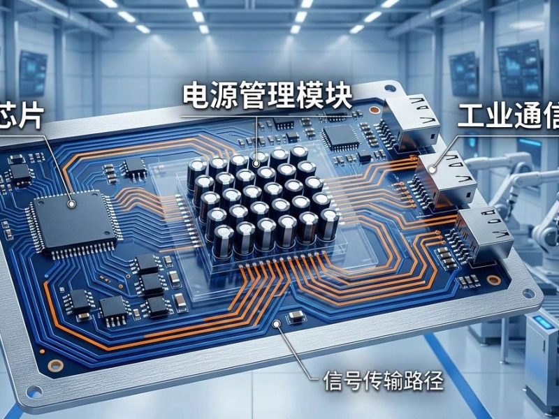
Unlocking Performance with High-Layer Count Industrial PCB SolutionsJune/15/2026
An Introduction to HDI Technology for Compact Industrial ElectronicsJune/16/2026

Innovative Industrial PCB Solutions for Renewable Energy SystemsAugust/11/2026
Material Selection Guide for High-Speed Industrial PCB SolutionsJuly/14/2026

Designing High-Frequency PCBs for Industrial 5G and IoT ApplicationsJune/26/2026

Overcoming Bend Radius Challenges in Flex PCB SolutionsAugust/14/2026