Open Nav


When a Pcb Design calls for 20, 24, or even 32 copper layers, you have moved decisively out of the territory of routine manufacturing. At this level of complexity, the fabrication process transforms from a relatively standardized production workflow into a bespoke engineering challenge where every layer, every via, and every material choice demands precise coordination. Industrial applications—military radar systems, medical imaging equipment, advanced networking hardware, and industrial power conversion systems—routinely require these high-layer-count boards because the signal routing density, Power Distribution complexity, and Impedance Control requirements simply cannot be achieved with fewer layers.
But building a reliable 20-plus layer PCB is genuinely difficult. The challenges are not merely additive—each additional layer compounds the complexity of alignment, Thermal Management, quality verification, and yield optimization in ways that make manufacturing yield drop sharply and process window tolerances tighten dramatically. Understanding these challenges helps engineers make better design decisions, procurement teams write more accurate specifications, and quality engineers build more effective inspection protocols.
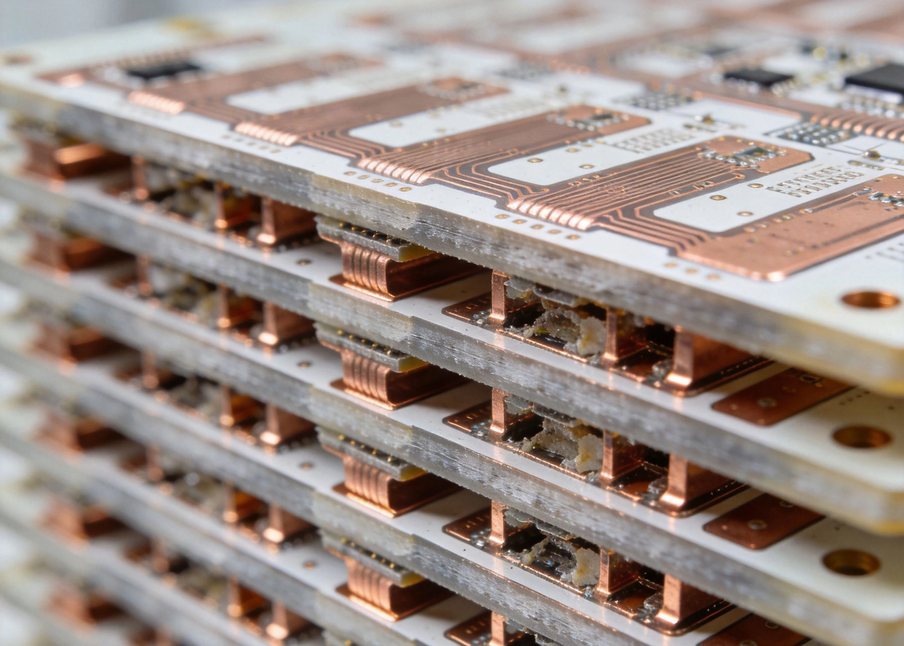
Before exploring the manufacturing difficulties, it is worth understanding why certain applications genuinely require such extreme layer counts rather than simply optimizing a simpler stack-up.
Military and aerospace systems often need separate dedicated layers for power bus distribution, ground planes, high-speed signal routing, and low-speed control signals, all isolated from each other to prevent crosstalk and electromagnetic interference. With systems that operate across dozens of functional modules, the layer budget fills up quickly. A typical military signal processing board might have 6 to 8 ground and power layers dedicated solely to distributing clean power and maintaining reference planes, with the remaining layers carrying signal traces.
Medical imaging equipment such as CT scanners, MRI machines, and ultrasound processors handle extremely high-bandwidth data streams that require Controlled Impedance routing on multiple differential pair layers. The density of data converters, FPGAs, and memory modules on these boards creates routing congestion that only additional layers can relieve without compromising Signal Integrity.
Industrial power conversion and motor control systems need Thick Copper layers for high-current bus bars, multiple isolation boundaries between high-voltage and low-voltage circuits, and dedicated layers for current sensing and feedback networks. The combination of power and signal requirements on a single board inevitably drives up the layer count.
Registration—the precise alignment of layers during lamination—is the single most critical and most difficult challenge in high-layer-count Pcb Manufacturing. As layer count increases, the cumulative registration error across all layers grows. If each individual layer can shift by 0.05 millimeters during lamination, a 24-layer board has 23 potential error accumulation points, and the worst-case misalignment between the top and bottom layers can approach or exceed what is acceptable for fine-pitch components.
Manufacturers address registration through multiple strategies. Target strips—small registration marks at the corners and edges of each layer—are optically aligned before lamination to minimize within-layer offset. However, this only controls the alignment before heat and pressure are applied. During lamination, the resin in the prepreg flows and exerts forces that can shift layers, especially in the center of large panels. Advanced manufacturers use Sequential Lamination builds, where subsets of layers are laminated together in stages rather than all at once, to limit the number of layers that can accumulate relative shift in any single step.
For the most demanding high-layer-count boards, blind and Buried Via structures are used strategically to reduce the number of layers that any single drill operation must penetrate, which indirectly reduces registration demands on via placement. However, this introduces its own set of manufacturing complexities.
Laminating 20 or more layers together in a single press cycle presents formidable challenges in void management. Voids—small pockets of air or volatiles trapped between layers—are unacceptable in high-reliability boards because they create Delamination risk, compromise the integrity of blind and buried vias, and can cause insulation failures between adjacent signal layers. As the number of prepreg layers increases, the total volatile content in the layup increases proportionally, and the pressure and temperature profile required to drive out all volatiles becomes more demanding.
Vacuum-assisted lamination is essentially mandatory for 20-plus layer builds. The panel is enclosed in a vacuum bag before being placed in the lamination press, which reduces the ambient pressure inside the layup and allows volatiles to escape more easily during the pressing cycle. Even with vacuum assistance, some manufacturers perform multiple lamination stages for very high layer counts, building the board in sub-assemblies of 8 to 10 layers that are then laminated together in a final stage. This incremental approach reduces void risk but adds processing steps, cost, and cycle time.
Material Selection matters enormously here. Low-flow prepregs reduce the risk of resin squeeze-out and trace displacement but require higher lamination pressure. High-flow prepregs fill gaps more easily but can cause resin starvation in other areas. The manufacturer's material engineering team must select the right prepreg/core combination for each specific stack-up configuration.
High-layer-count boards absorb and conduct heat differently from thin boards during the multiple thermal cycles they endure: lamination, soldering, and any rework or repair. The thick, dense construction of a 24-layer board means that heat penetrates slowly during solder reflow, which can lead to incomplete solder joints on bottom-side components if the profile is not adjusted for the board's thermal mass. Conversely, uneven heating during lamination can create internal stresses that cause warpage after the board cools.
Warpage control is particularly challenging for asymmetric stack-ups—designs where the layer distribution is not balanced around the neutral axis of the board. A board with 14 layers on the top half and 10 on the bottom half will naturally want to warp toward the heavier side as it cools from the lamination temperature. Manufacturers counteract this through controlled cooling ramps, back-to-back pressing arrangements in the lamination press, and in some cases, adding compensating dummy layers or copper weights to balance the stack-up.
For the designer, keeping the stack-up symmetric around the neutral axis is one of the most impactful decisions you can make to reduce warpage and simplify manufacturing. An asymmetric 24-layer stack-up is significantly more difficult to produce reliably than a symmetric 24-layer design, even if both are electrically equivalent.
Through-hole drilling on a 24-layer board with 2-ounce or 3-ounce copper layers is a mechanical challenge that pushes drilling equipment to its limits. The drill bit must penetrate and clear material from up to 5 or 6 millimeters of total thickness, including copper plating on the hole walls from inner layers. As drill depth increases, drill wander—the tendency of the bit to deflect sideways as it enters the material—increases proportionally. Drill wander beyond 0.05 millimeters on a 2.0-millimeter finished hole is unacceptable for most high-reliability specifications, and maintaining this tolerance on a deep stack requires carbide drill bits, optimized spindle speeds, and precise hit-point accuracy from the CNC drilling machine.
Blind and buried vias add another layer of complexity. A Blind Via that connects layer 1 to layer 4 must be drilled before the outer layers are laminated onto the sub-assembly. A Buried Via between layers 8 and 12 must be drilled and plated in a sub-panel that is later buried inside the final stack. Each via type requires a specific stage in the manufacturing sequence, and every additional via generation increases the number of processing steps, the risk of contamination between steps, and the cumulative registration budget.
The aspect ratio of through-holes—the ratio of board thickness to finished hole diameter—directly affects plating quality. Aspect ratios above 10:1 are challenging; above 15:1 they become extremely difficult. High-layer-count boards naturally have higher aspect ratios for their through-holes. Designers who can tolerate larger minimum via sizes will dramatically improve manufacturing yield and reduce cost. A design that can use 0.5-millimeter minimum via size instead of 0.3 millimeters makes a substantial difference in the manufacturing feasibility of a 20-plus layer board.
Copper electroplating inside deep, narrow holes is governed by the same electrochemical throwing power limitations that affect all PCB plating, but at extreme aspect ratios, the challenges become critical. The plating solution must penetrate all the way to the bottom of a hole that may be 4 or 5 millimeters deep and only 0.4 millimeters in diameter. If the agitation of the plating solution is insufficient or the current density is too high, the top of the hole receives excess copper while the bottom receives too little, creating a conformal rather than uniform plating profile.
Void-free plating inside high aspect ratio holes requires pulse-reverse plating techniques, where the current direction alternates periodically to help fresh solution reach the hole bottom and prevent the accumulation of "drag-out" copper that can seal the hole entrance before the interior is fully plated. Specialized plating additives that improve throwing power are essential for these applications, and the plating bath chemistry must be monitored and maintained with exceptional rigor.
For boards that will undergo multiple thermal cycles in service, the ductility of the plated copper is as important as its thickness. Brittle copper—caused by high current density plating or contaminated bath chemistry—cracks under the thermal expansion and contraction stress that occurs every time the board powers on and heats up. Boards that will see thousands of power cycles must have copper barrel elongation exceeding 15 percent to survive without developing intermittent opens.
Achieving Controlled Impedance on a single-layer or dual-layer board is straightforward—trace width, trace thickness, and dielectric thickness between the trace and its reference plane determine the impedance, and these parameters are relatively easy to control. On a 24-layer board, the challenge multiplies because every signal layer has a different dielectric thickness to its nearest reference plane, and the presence of adjacent signal layers, ground slots, and thermal relief patterns creates parasitic capacitance and inductance that shift the effective impedance.
Signal Integrity engineers must account for crosstalk between adjacent signal layers, the effect of antipad anti-pads—the openings in reference planes around through-hole vias—on trace impedance, and the coupling between traces on different layers that cross over each other. Full-wave electromagnetic simulation is effectively mandatory for 20-plus layer designs where controlled impedance is a requirement, and the manufacturing stack-up must be held to tight tolerances on both Dielectric Constant and thickness to deliver the predicted impedance in the finished board.
Inspecting and testing a 24-layer board is an order of magnitude more complex than testing a 6-layer board, and the inspection methods that work for lower-layer-count boards are often insufficient for high-layer-count builds.
Cross-sectioning—the process of cutting a sample board, mounting it in epoxy, polishing it to a mirror finish, and examining it under a microscope—is the definitive method for verifying internal structure quality. It reveals void location and size, copper plating thickness on hole walls, dielectric thickness between layers, and any Delamination or contamination at layer interfaces. For 20-plus layer boards, multiple cross-sections are taken at strategic locations: corner, center, and edge of the panel, and sometimes at specific feature locations where the risk of defect is highest.
p>Cross-sectioning is destructive—once a board is sectioned, it cannot be used—which means manufacturers must balance the number of cross-section samples against the number of good boards they can deliver. For production runs, a statistical sampling plan is used, where a defined percentage of boards from each lot are cross-sectioned as qualification samples.Aoi works well for surface defects on outer layers but cannot see inside the board. For inner layers, automated optical inspection verifies that the etched inner layer patterns are correct before lamination, but once the board is assembled, Aoi is blind to everything except the outer surfaces. For high-layer-count boards, this means AOI must be performed at multiple stages during manufacturing—after each inner layer etch, after each lamination stage, and after outer layer processing—which adds time and cost but does not provide complete confidence in the final assembled board.
Flying Probe Testing checks electrical connectivity between nets by driving current through Test Points on the board surface. On a high-layer-count board, test point access becomes a design constraint—your design must include sufficient Test Points to probe all the nets on all layers, which can consume board area and complicate routing. Micro-via test pads are often used to access buried layer nets, but this requires additional design consideration.
For boards with internal nets that have no surface access point, Flying Probe Testing cannot fully verify connectivity. In these cases, cross-sectioning at selected locations provides some verification of internal layer connections, but it is inherently a sampling-based approach rather than a comprehensive test.
X-ray Inspection reveals hidden features inside the board, including the quality of solder joints on BGA components, the fill quality of blind and buried vias, and any voids or delamination visible in the cross-sectional plane. For 20-plus layer boards with complex via structures, X-ray Inspection is an essential quality tool that complements cross-sectioning by providing non-destructive verification of internal features across 100 percent of the boards in a lot rather than relying on statistical sampling.
Design decisions made at the schematic and layout stage have an outsized impact on the manufacturability and cost of high-layer-count boards. Following these guidelines will significantly improve your chances of a successful build.
Commercially manufactured PCBs with controlled quality systems are routinely built up to 32 layers. Beyond that, specialized manufacturers can produce boards with 40, 48, or even more layers, but the number of qualified suppliers drops significantly and pricing increases substantially. For most industrial applications, a 20 to 32 layer range covers the vast majority of requirements while remaining within the capability of experienced high-layer-count manufacturers.
The cost premium for high-layer-count boards reflects both the complexity of the process and the yield impact of that complexity. Every additional layer adds processing steps: inner layer processing, lamination cycles, additional drill operations, and more inspection stages. More importantly, the yield for very high layer counts drops compared to standard boards because the probability of at least one layer registration error, void, or plating defect increases with layer count. A manufacturer who achieves 95 percent yield on a 6-layer board might achieve 75 percent yield on a 24-layer board, and the lost material cost is distributed across the surviving boards.
Sequential Lamination is a process where the board is built up in multiple lamination stages rather than all layers being pressed together in a single cycle. For example, a 24-layer board might be built in three stages: layers 1 through 8 are laminated first, layers 9 through 16 are laminated as a separate sub-assembly, and then these two sub-assemblies are laminated together with layers 17 through 24 in a final press. Sequential lamination reduces void risk, improves registration for buried layer features, and is essentially mandatory for very high layer counts. It also adds cost and cycle time.
Impedance Control is verified through a combination of design simulation, process control, and measurement. During design, full-wave electromagnetic simulation predicts the impedance based on the specified stack-up and trace geometry. During manufacturing, the dielectric thickness and copper thickness are controlled through process parameters and verified by cross-sectioning test coupons from each panel. Impedance test coupons—traces with specific controlled geometry built into the panel frame—are measured using Time Domain Reflectometry (TDR) to verify that the actual impedance matches the design target.
Lead times for 20-plus layer boards vary significantly based on the manufacturer's order book, the complexity of your design, and the quality class required. Standard 20 to 24 layer boards with IPC Class 2 requirements typically take 10 to 15 business days for fabrication. Boards with complex blind/buried via structures, Ipc Class 3 requirements, or specialty materials may require 20 to 30 business days. Always request a firm lead time quote from your manufacturer when placing an order with these complexity levels.
Manufacturing 20-plus layer industrial PCBs sits at the intersection of advanced materials science, precision engineering, and rigorous process control. Every step of the manufacturing pipeline—inner layer processing, stack-up preparation, lamination, drilling, plating, and inspection—operates under tighter tolerances and demands more careful execution than standard PCB production. The challenges of layer registration, void management, deep-hole plating, thermal warpage control, and impedance consistency are not insurmountable, but they require a manufacturer with deep experience, sophisticated equipment, and mature quality systems.
For engineers and procurement specialists specifying high-layer-count boards, the key takeaway is that your design decisions have an enormous influence on manufacturing success. Symmetric stack-ups, appropriate minimum feature sizes, strategic via usage, and comprehensive documentation all dramatically improve the probability of a successful build. Working closely with your manufacturer during the design phase—sharing stack-up details, discussing via strategies, and submitting files for Dfm Review—catches potential problems before they consume material and cycle time.
When done right, a 20-plus layer PCB is a triumph of engineering precision—a board that reliably carries hundreds of signals, distributes power across multiple rails, and maintains controlled impedance through the most demanding operating environments. Getting there requires investment in design best practices and a trusted manufacturing partner, but the result is a board that performs at the level your industrial application demands.
This article is provided for general informational purposes regarding high-layer-count Pcb Manufacturing challenges. Specific manufacturing capabilities, yield rates, and lead times vary by supplier. Always consult directly with your manufacturing partner for design-specific guidance.
Via-in-Pad and Microvias: Key Features of Advanced HDI SolutionsJuly/26/2026
Heavy Copper PCBs: The Solution for High-Current Industrial ApplicationsJune/18/2026

Cost Analysis: Is Rigid-Flex the Right Solution for Your Industrial Project?September/15/2026
Manufacturing Processes Unique to Rigid-Flex PCB SolutionsOctober/10/2026
Overcoming Bend Radius Challenges in Flex PCB SolutionsAugust/14/2026
Aluminum vs. Copper Base: Choosing the Best Metal Core SolutionJuly/29/2026
Unlocking Performance with High-Layer Count Industrial PCB SolutionsJune/15/2026
Minimizing Signal Loss and Crosstalk in High-Speed PCB LayoutsSeptember/01/2026