Open Nav


The Industrial Electronics landscape is undergoing a dramatic transformation as applications become increasingly complex and performance requirements continue to escalate. From advanced robotics and Industrial Automation to sophisticated medical equipment and aerospace systems, the demand for high-performance circuit boards has never been greater. High-layer Count Industrial Pcb solutions have emerged as the answer to these challenges, offering unprecedented capabilities that enable engineers to push the boundaries of what's possible in Industrial Electronics. This comprehensive guide explores how High-layer Count PCBs are unlocking new levels of performance in industrial applications and provides practical insights for engineers and decision-makers looking to leverage this technology.
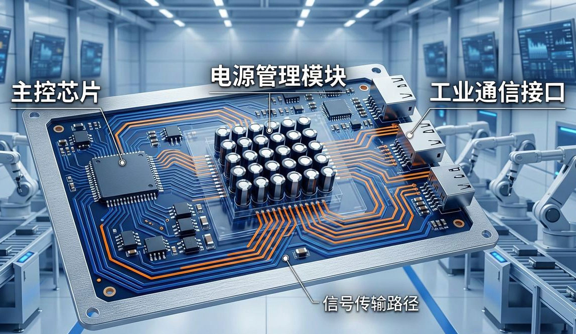
High-layer count printed circuit boards represent the pinnacle of PCB technology, featuring ten or more conductive layers that enable complex circuit designs with exceptional performance characteristics. These sophisticated assemblies provide the foundation for modern industrial electronics that require high functionality in compact form factors. Unlike traditional double-sided or four-layer boards, high-layer count PCBs offer increased routing density, enhanced Signal Integrity, superior Power Distribution, and improved electromagnetic compatibility - all essential for demanding industrial applications.
The evolution of High-layer Count Pcb technology has been driven by several key factors. First, the increasing complexity of industrial systems requires more functions and features to be integrated into smaller packages. High-layer count boards enable this integration by providing additional routing channels and dedicated layers for power, ground, and signal separation. Second, the need for higher operating frequencies and faster signal speeds has created demand for improved Signal Integrity characteristics that multi-layer boards naturally provide through Controlled Impedance and reduced crosstalk. Third, industrial applications often require robust Power Distribution systems that can handle high currents while maintaining stable voltages - a capability that high-layer count PCBs excel at through dedicated power and ground planes.
Manufacturing high-layer count PCBs requires specialized expertise and advanced fabrication capabilities. As layer count increases, the complexity of alignment, registration, and lamination processes grows exponentially. Modern HDI (High Density Interconnect) techniques often combine with high-layer count designs to achieve even greater functionality in smaller packages. The synergy between Hdi Technology and multi-layer designs enables the creation of boards that feature Microvias, buried vias, and Blind Vias - all of which contribute to enhanced performance and miniaturization capabilities.
The cost structure of high-layer count PCBs differs significantly from simpler boards. While the upfront manufacturing costs are higher, the total cost of ownership often proves lower when considering factors like reduced board count, simplified assembly, improved reliability, and enhanced performance. For many industrial applications, the performance benefits of high-layer count boards far outweigh the additional manufacturing costs, making them the preferred choice for mission-critical systems.
High-layer count industrial PCBs have found extensive adoption across a wide range of demanding applications where performance, reliability, and functionality are paramount. These sophisticated circuit assemblies enable engineers to develop systems that would be impossible with traditional PCB technologies, opening new possibilities across various industrial sectors.
Industrial Automation and robotics represent one of the most significant application areas for high-layer count PCBs. Modern robotic systems require complex control electronics, advanced sensing capabilities, sophisticated motor drives, and real-time data processing - all of which benefit tremendously from multi-layer PCB technology. The increased routing density allows integration of multiple control functions on a single board, while dedicated power planes provide clean, stable power distribution to precision motion control systems. Additionally, the enhanced signal integrity characteristics ensure reliable operation of high-speed communication interfaces between robot controllers and peripheral equipment.
Medical electronics and diagnostic equipment represent another critical application domain. Medical devices must meet stringent requirements for reliability, accuracy, and electromagnetic compatibility while often operating in challenging environments. High-layer count PCBs enable the integration of complex analog and digital circuits in compact form factors, essential for portable medical devices and imaging equipment. The ability to separate sensitive analog signals from noisy digital circuits through dedicated layers and ground planes helps maintain the accuracy required for medical measurements and diagnostics.
Aerospace and defense applications leverage High-layer Count Pcb technology for mission-critical systems that must operate reliably under extreme conditions. Avionics, guidance systems, communication equipment, and radar systems all benefit from the enhanced performance capabilities of multi-layer boards. The robust construction of high-layer count PCBs provides superior mechanical stability and resistance to vibration and thermal stress - essential characteristics for aerospace applications. Furthermore, the electromagnetic shielding provided by multiple ground planes helps ensure electromagnetic compatibility in sensitive electronic environments.
Industrial computing and control systems also benefit significantly from high-layer count PCB solutions. Modern industrial computers, PLCs (Programmable Logic Controllers), and complex sensor interfaces require dense integration of processing, memory, and communication functions. High-layer count boards enable this integration while maintaining signal integrity across high-speed interfaces. The dedicated power distribution layers help maintain stable voltages across complex digital systems, ensuring reliable operation in industrial environments with varying power quality.
The benefits of high-layer count industrial PCBs extend beyond specific applications to include several overarching advantages:
Designing high-layer count industrial PCBs requires careful consideration of numerous factors that affect performance, manufacturability, and cost. Engineers must balance competing requirements while ensuring that the final design meets all performance specifications and quality standards. Understanding these design considerations is essential for successful implementation of high-layer count PCB solutions.
Layer stackup design represents one of the most critical aspects of multi-layer PCB development. The arrangement of signal, power, and ground layers significantly impacts signal integrity, power distribution, and overall board performance. Effective layer stackups typically follow several principles: signal layers should be adjacent to ground planes to provide proper return paths and minimize crosstalk; power and ground planes should be placed close together to create distributed decoupling capacitance; and sensitive signals should be isolated from noisy circuits through strategic layer placement. The choice between even and odd layer counts also affects manufacturing costs and complexity - even layer counts are generally preferred for balanced copper distribution and symmetrical construction.
Impedance Control becomes increasingly important as signal speeds increase in industrial applications. High-layer count PCBs enable proper impedance control through careful selection of dielectric materials, trace geometries, and reference plane configurations. Engineers must calculate characteristic impedance for high-speed signals based on trace width, thickness, dielectric thickness, and material properties. For differential signals, both single-ended and differential impedance must be controlled to ensure proper termination and signal integrity. Advanced field solvers and simulation tools help engineers optimize impedance characteristics before committing to fabrication.
Via selection and placement significantly affect both performance and manufacturability of high-layer count boards. The choice between through-hole vias, Blind Vias, and buried vias depends on design requirements and cost considerations. Through-hole vias provide the lowest cost but take up more space and can create discontinuities in reference planes. Blind and buried vias save space and maintain reference plane continuity but increase manufacturing complexity and cost. Via stubs must be considered for high-speed signals, as these can cause impedance discontinuities and signal reflections. For very high-frequency applications, techniques like back-drilling or Via-in-pad may be necessary to eliminate via stubs.
Material Selection for high-layer count industrial PCBs requires careful evaluation of electrical, thermal, and mechanical properties. Standard FR-4 materials work well for many applications up to several gigahertz, but high-frequency applications may require specialized materials with more stable dielectric properties. Key material characteristics to consider include Dielectric Constant (Dk), dissipation factor (Df), Thermal Conductivity, coefficient of thermal expansion (CTE), and moisture absorption. Hybrid constructions using different materials for different layers can optimize performance and cost for specific applications.
Design For Manufacturability (DFM) becomes increasingly important as layer count increases. Complex multi-layer designs must balance performance requirements with practical manufacturing considerations. Key DFM aspects include maintaining adequate clearance between copper features, ensuring proper annular ring sizes for vias, avoiding acute angles in traces, providing adequate panel utilization, and following fabricator design rules for minimum trace width, spacing, and drill sizes. Early collaboration with PCB fabricators helps ensure that designs are manufacturable and cost-effective.
Thermal Management becomes more critical in high-layer count boards due to the increased component density and power dissipation. Multiple copper layers provide improved heat spreading capabilities, but designers must still consider thermal requirements carefully. Techniques like Thermal Vias, copper pours, and proper component placement help manage Heat Dissipation. For Power Electronics applications, specialized thermal management techniques like metal-core PCBs or embedded heat sinks may be necessary.
Manufacturing high-layer count industrial PCBs presents unique challenges that require specialized equipment, processes, and expertise. As layer count increases, the complexity of fabrication processes grows exponentially, requiring careful attention to detail and sophisticated Quality Control systems. Understanding these manufacturing challenges helps engineers design boards that are both high-performing and manufacturable.
Alignment and registration represent perhaps the most critical challenge in multi-layer Pcb Manufacturing. Each additional layer increases the complexity of maintaining proper alignment between layers, as small misalignments can accumulate across multiple lamination cycles. Modern manufacturers address this challenge through advanced alignment systems using optical targets, sophisticated imaging systems, and tight process controls. The choice between subtractive and additive processes also affects registration - additive processes generally provide better registration for very high-density designs.
Lamination complexity increases significantly with layer count. Multiple lamination cycles are often required for boards with more than 12-16 layers, and each lamination cycle introduces potential defects like voids, Delamination, or resin flow issues. Manufacturers address these challenges through optimized lamination parameters, advanced press equipment with precise temperature and pressure control, and comprehensive Material Selection processes that ensure compatibility between different laminate materials.
Drilling challenges multiply as layer count increases. Deeper boards require more drilling passes, more sophisticated drill bits, and more complex drill programs. Drill bit deflection becomes more significant with deeper holes, potentially affecting hole location accuracy and wall quality. Advanced drilling equipment with rigid spindles, high-rpm capabilities, and sophisticated drill bit selection helps address these challenges. For very high-density designs, Laser Drilling may be necessary for Microvias.
Plating uniformity becomes more challenging with high-aspect-ratio holes in thick multi-layer boards. Ensuring proper copper plating throughout deep vias requires optimized plating chemistry, advanced plating equipment with proper agitation, and careful process control. Inadequate plating can cause reliability issues, particularly in high-current applications or environments with Thermal Cycling. Manufacturers use techniques like pulse plating and reverse pulse plating to improve plating quality in high-aspect-ratio holes.
Quality Control and inspection become more complex with high-layer count boards. Many critical features are not visible from the surface, requiring specialized inspection techniques like X-ray Inspection for buried and blind vias, cross-sectional analysis for plating quality verification, and impedance testing for signal integrity verification. Automated optical inspection (Aoi) systems with high-resolution cameras help detect surface defects, while electrical testing ensures proper electrical characteristics. Manufacturers implement comprehensive quality systems with statistical process control to maintain consistent quality across production runs.
Cost considerations play a significant role in high-layer count Pcb Manufacturing. Additional layers increase material costs, processing time, and yield risk. Manufacturers address these challenges through optimized panel utilization, efficient process sequencing, and advanced automation to reduce labor costs. Close collaboration between design and manufacturing teams helps optimize designs for cost-effective manufacturing while maintaining performance requirements.
The field of high-layer count Industrial Pcb technology continues to evolve rapidly, driven by advancing application requirements and emerging manufacturing technologies. Several key trends are shaping the future of Industrial Pcb solutions, offering new capabilities and opportunities for engineers and manufacturers.
Increased layer counts continue to push the boundaries of what's possible in industrial electronics. Boards with 20-30 or more layers are becoming increasingly common for the most demanding applications, enabling unprecedented integration levels and performance characteristics. This trend requires advances in materials, processes, and equipment to maintain manufacturability and reliability at higher layer counts.
HDI (High Density Interconnect) techniques are increasingly being combined with high-layer count designs to achieve even greater functionality in smaller packages. Microvias, Sequential Lamination, and advanced via technologies enable designers to maximize routing density while maintaining performance characteristics. The combination of HDI and multi-layer technologies is particularly valuable for portable industrial devices and applications where space is at a premium.
Advanced materials continue to expand the capabilities of high-layer count industrial PCBs. New laminate materials with improved high-frequency characteristics, better thermal performance, and enhanced reliability enable new applications in areas like automotive radar, industrial imaging, and high-speed computing. Hybrid constructions using different materials for different layers allow optimization of performance and cost for specific applications.
Embedded component technology represents an emerging trend that's gaining traction in industrial applications. Embedding passive components like resistors and capacitors within PCB layers reduces overall size, improves performance, and increases reliability. This technology is particularly valuable for high-frequency applications where parasitic effects of surface mount components can affect performance.
Advanced manufacturing techniques like additive manufacturing and laser direct structuring are opening new possibilities for Industrial Pcb Production. These technologies enable rapid prototyping, reduced material waste, and the creation of complex three-dimensional structures that would be difficult or impossible with traditional subtractive processes. While currently limited in resolution and speed compared to traditional manufacturing, these techniques continue to advance and may play an increasingly important role in future Industrial Pcb Production.
Design automation tools continue to evolve, making it easier for engineers to design complex high-layer count PCBs. Advanced simulation capabilities, automated routing algorithms, and integrated Design For Manufacturability tools help engineers optimize designs for performance, reliability, and manufacturability. These tools reduce design time and help avoid common pitfalls that can affect product quality and time-to-market.
Sustainability concerns are driving developments in environmentally friendly PCB manufacturing processes. Lead-free solders, halogen-free materials, and energy-efficient manufacturing processes are becoming increasingly important as environmental regulations become more stringent and customers demand more sustainable products. Manufacturers are developing new processes and materials that maintain performance while reducing environmental impact.
High-layer count Industrial Pcb solutions have become essential for enabling the advanced capabilities required by modern industrial electronics. From industrial automation and robotics to medical equipment and aerospace systems, these sophisticated circuit assemblies provide the foundation for pushing the boundaries of performance, functionality, and reliability. As application requirements continue to become more demanding, the importance of high-layer count PCB technology will only increase.
Success in implementing high-layer count PCB solutions requires careful consideration of design requirements, manufacturing capabilities, and cost trade-offs. Engineers must balance competing factors like performance, reliability, manufacturability, and cost while ensuring that designs meet all application requirements. Collaboration between design teams, manufacturers, and material suppliers is essential for optimizing solutions for specific applications.
The future of high-layer count industrial PCB technology looks bright, with continued advances in materials, processes, and design tools enabling even greater capabilities. Organizations that invest in understanding and leveraging these technologies will be well-positioned to develop the next generation of industrial electronics products that meet evolving market demands.
As the industrial electronics landscape continues to evolve, high-layer count PCB solutions will remain at the forefront of enabling new capabilities and applications. By understanding the technology, its benefits, and its implementation considerations, engineers and decision-makers can make informed decisions about when and how to leverage this powerful technology for their specific applications.
While definitions can vary, boards with 10 or more layers are generally considered high-layer count PCBs. However, the threshold depends on application context and industry standards. For industrial applications, boards with 12-16 layers are common for complex systems, while the most demanding applications may require 20-30 or more layers. The choice of layer count depends on factors like routing density, power requirements, signal integrity needs, and cost considerations.
High-layer count PCBs offer several key advantages including enhanced signal integrity through proper impedance control and reduced crosstalk, improved power distribution with dedicated power and ground planes, increased functionality through higher routing density, better thermal management with multiple copper layers, and superior mechanical stability. These advantages enable more complex, high-performance designs in smaller form factors compared to simpler PCB configurations.
The primary manufacturing challenges include maintaining alignment and registration across multiple layers, managing lamination complexity for multiple build-up cycles, achieving consistent plating in high-aspect-ratio holes, drilling deep holes accurately without drill bit deflection, implementing comprehensive quality control for hidden features, and managing increased costs. Addressing these challenges requires specialized equipment, advanced processes, and experienced manufacturing personnel.
High-layer count PCBs have significantly higher upfront manufacturing costs due to increased material usage, longer processing times, and lower yields. However, total cost of ownership often proves lower when considering reduced board count, simplified assembly, improved reliability, enhanced performance, and time-to-market advantages. For many industrial applications, the performance benefits outweigh the additional manufacturing costs, making multi-layer boards the preferred choice for mission-critical systems.
Engineers should consider high-layer count PCBs when applications require high routing density in limited space, high-speed digital signals with Controlled Impedance, complex power distribution requirements, superior signal integrity and electromagnetic compatibility, integration of multiple functions in compact packages, or operation in demanding environments with strict reliability requirements. The decision should balance performance requirements against cost and manufacturing complexity considerations.
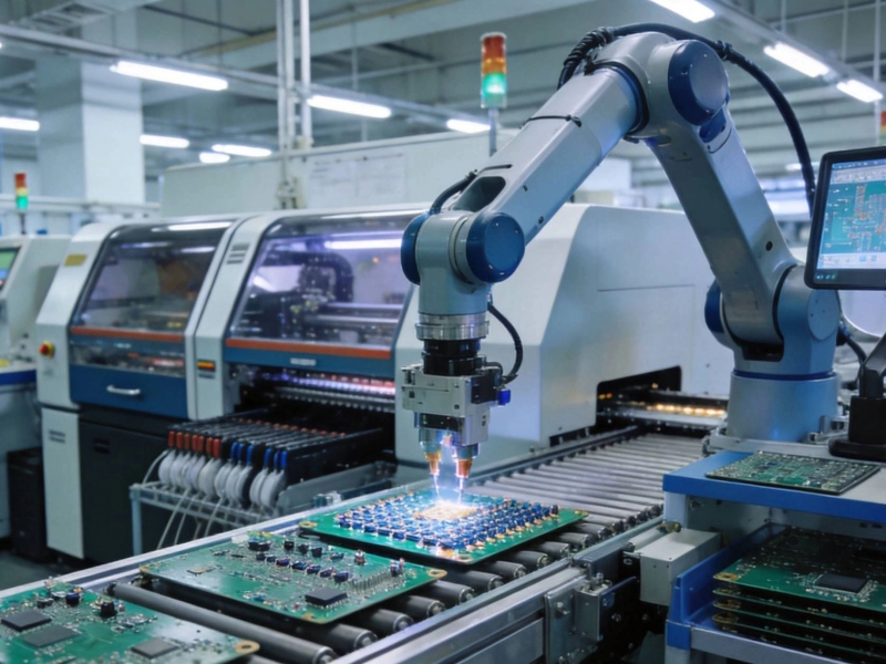
End-to-End Industrial PCB Solutions: From Design to DeliveryJuly/08/2026
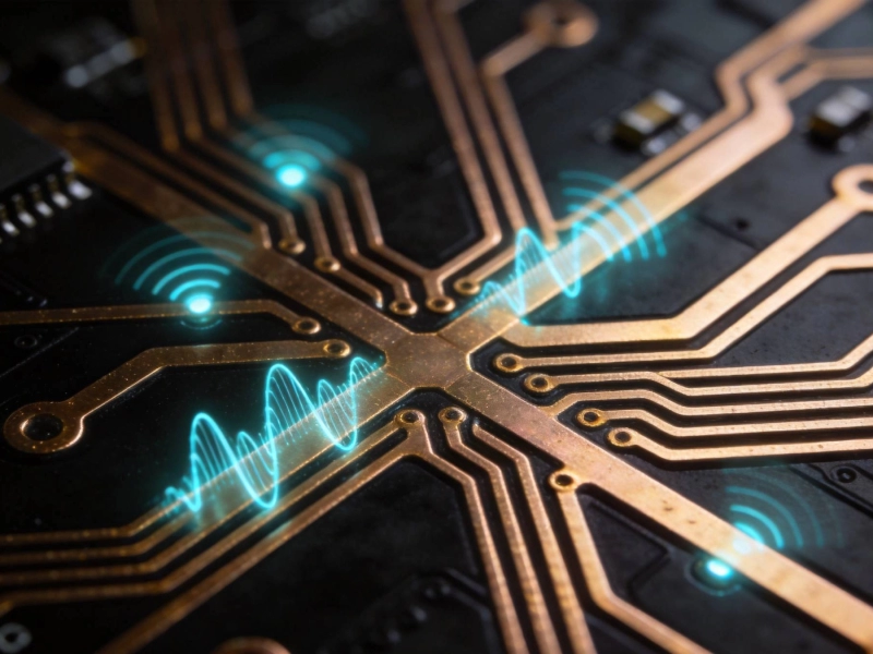
Designing High-Frequency PCBs for Industrial 5G and IoT ApplicationsJune/26/2026
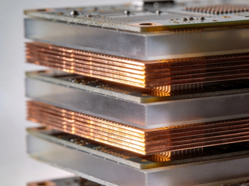
Stack-up Design Strategies for High-Layer Count Industrial PCBsOctober/09/2026
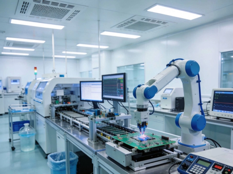
Tailored Industrial PCB Solutions for Medical Device ManufacturersJune/12/2026
Rogers vs. PTFE: Comparing Materials for High-Frequency SolutionsSeptember/17/2026
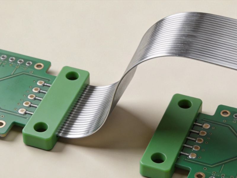
Reducing Weight and Space with Rigid-Flex Industrial PCB SolutionsJuly/28/2026
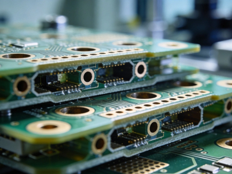
Via-in-Pad and Microvias: Key Features of Advanced HDI SolutionsJuly/26/2026
How Heavy Copper Solutions Improve Reliability in Motor DrivesSeptember/16/2026