Open Nav


Industrial environments demand electronics that can withstand extreme Thermal Cycling, mechanical vibration, and continuous high-power operation without failing. When designing for sectors like renewable energy inverters, heavy machinery automation, or medical imaging, standard two-layer boards simply do not cut it. Engineers require multi-layer architectures to manage dense signal routing while maintaining robust Power Distribution. But how do manufacturers reliably build these complex, high-layer-count boards?
This article dives deep into the advanced techniques in multi-layer industrial PCB Fabrication. We will explore the engineering realities behind High-Density Interconnect (HDI) designs, precision lamination processes, and the stringent testing protocols required to guarantee mission-critical reliability.
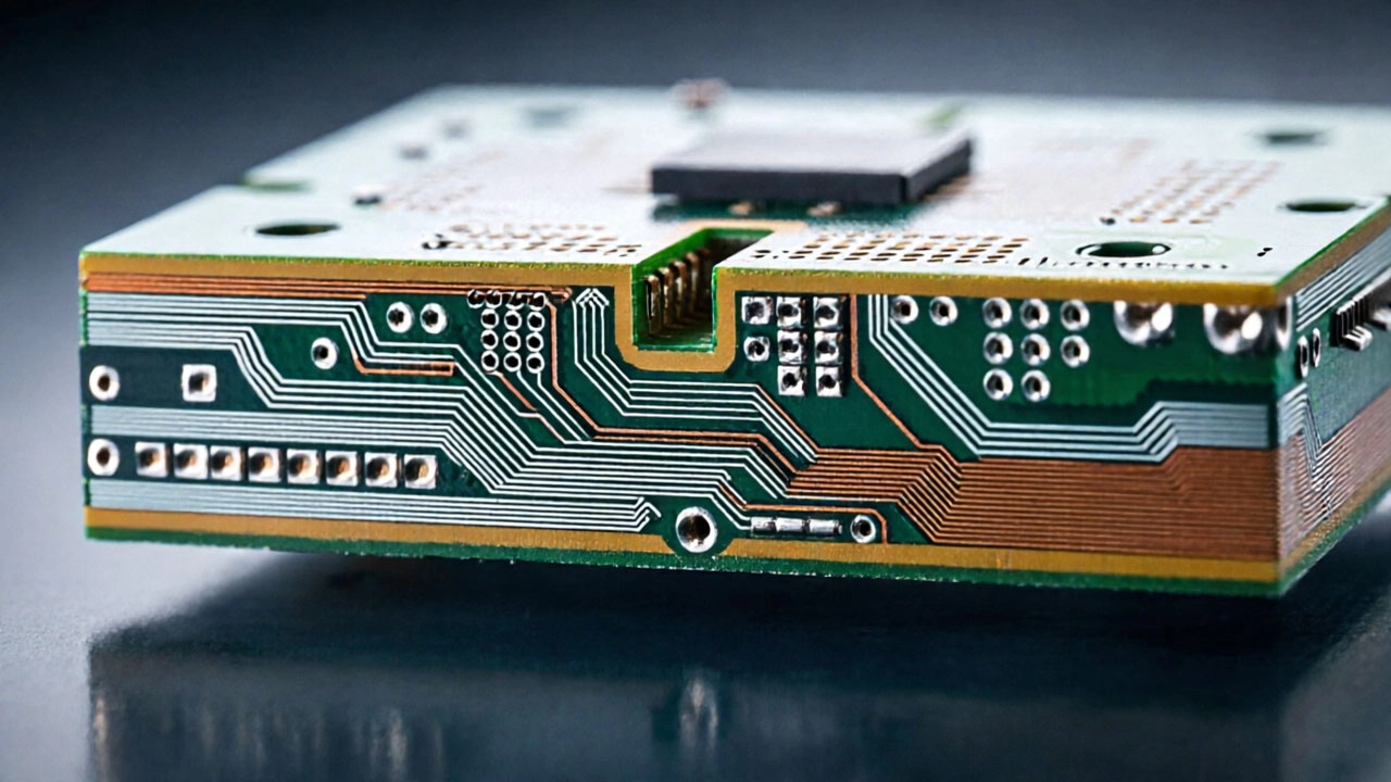
As industrial controllers become more compact and powerful, maximizing board real estate is paramount. High-Density Interconnect (HDI) technology achieves this through advanced micro-via structures and sequential lamination.
Practical Takeaway: If your design requires HDI, engage your fabricator during the schematic phase. Laser drill capabilities and via fill options vary significantly between factories. Early Design For Manufacturing (DFM) alignment prevents costly respins later.
The heart of any multi-layer board is its core. For industrial applications handling high voltages or high-frequency signals, material consistency is non-negotiable.
From my experiance reviewing Failure Analysis reports, I've seen that many field failures in harsh environments trace back to poor lamination quality. Voids or Delamination inside the board act as thermal insulators, causing localized hot spots that eventually destroy the assembly.
You cannot inspect what you cannot see. Once a 24-layer board is laminated, internal defects are hidden forever unless caught by advanced diagnostic tools.
Beyond structural validation, electrical integrity is verified through High-Potential (Hi-Pot) testing to ensure sufficient isolation between high-voltage planes. Automated Flying Probe testers verify net connectivity at millions of points per hour, while Time Domain Reflectometry (TDR) confirms that Controlled Impedance traces meet exact specifications.
Fabricating multi-layer industrial PCBs is a symphony of material science, precision mechanics, and rigorous statistical process control. Success requires moving beyond basic Gerber translation to true engineering collaboration. By leveraging HDI technologies, mastering lamination dynamics, and enforcing uncompromising QA standards, manufacturers deliver boards that keep critical infrastructure running flawlessly.
Planning a complex Industrial Pcb project? Don't leave your board's reliability to chance. Contact our engineering team today to discuss your stack-up requirements and leverage our advanced fabrication capabilities for your next critical deployment.
Q1: What is the maximum layer count currently achievable in mass production?
While prototyping labs can push beyond 40 layers, reliable mass production for industrial applications typically peaks around 24 to 32 layers. Beyond this, yield rates drop exponentially due to alignment tolerances and lamination complexity.
Q2: How do you prevent via cracking in thick-copper industrial boards?
Via cracking is usually caused by the Coefficient of Thermal Expansion (CTE) mismatch between copper and FR4. Using High-tg Materials, selecting resins with lower Z-axis CTE, and employing rigid-flex transitions can dramatically improve Thermal Fatigue resistance.
Q3: Is Impedance Control necessary for all multi-layer industrial boards?
Not necessarily. However, if your board handles communication protocols like Ethernet, CAN bus, or PCIe, strict impedance control is mandatory. Even for power boards, managing return paths and minimizing loop inductance through proper Stack-up Design is crucial for EMC compliance.

Eco-Friendly Practices in Modern Industrial PCB FabricationSeptember/20/2026
Precision Engineering: Tolerances in High-End Industrial PCB FabricationSeptember/03/2026
Materials, Methods, and Industry Standards ExplainedMay/27/2026
The Impact of Surface Finishes on Industrial PCB Fabrication QualityJuly/16/2026
Predicting Lifespan: Accelerated Life Testing for Industrial PCB ReliabilityAugust/03/2026
Overcoming Common Defects in Industrial PCB FabricationAugust/03/2026
How to Choose the Right Manufacturer for Industrial PCB FabricationJune/29/2026
The Role of Laser Drilling in High-Precision Industrial PCB FabricationOctober/15/2026