Open Nav


Whether you're an electronics engineering student, a product designer, or someone breaking into the PCB industry, understanding the fundamentals of industrial PCB Fabrication is essential. This guide breaks down everything you need to know about Pcb Materials, the core manufacturing methods, and the industry standards that ensure quality and consistency across the global Electronics Supply Chain.
Printed circuit boards are everywhere—from the device you're reading this on to the car you drive and the medical equipment that saves lives. Yet few people understand what goes into making these critical components. Industrial PCB Fabrication is a sophisticated process that transforms raw materials into the interconnected platforms that power modern technology.
This beginner-friendly guide covers the three pillars of Pcb Fabrication knowledge: the materials that form the foundation, the methods that shape the final product, and the standards that guarantee quality. By the end, you'll have a solid grasp of how professional PCBs are made and why certain choices matter.
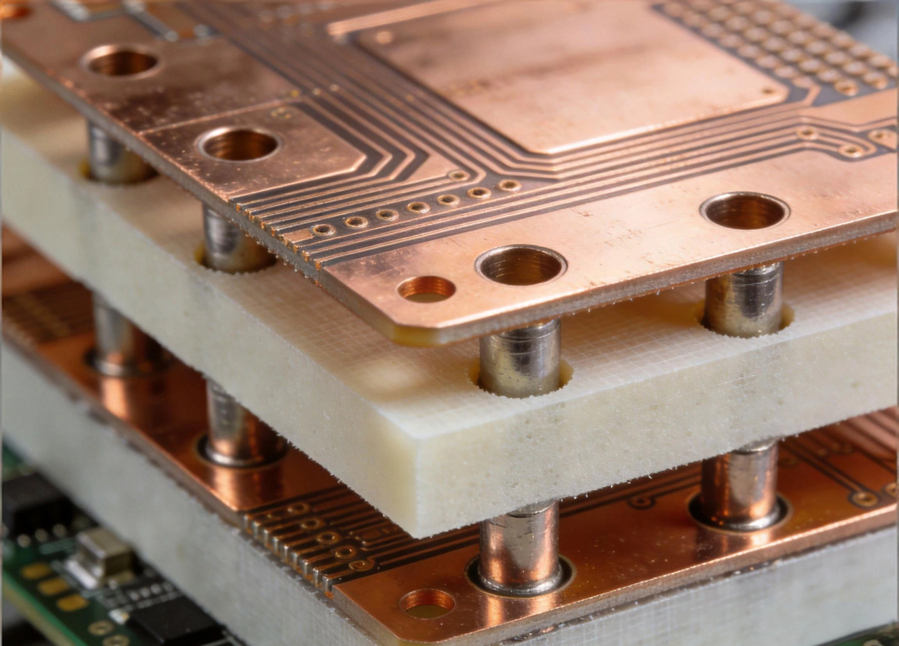
The materials used in Pcb Fabrication determine a board's electrical performance, mechanical durability, thermal characteristics, and cost. Choosing the right substrate and copper is often the first critical decision in any PCB project.
The substrate is the non-conductive base material that supports the copper circuitry. Its properties directly influence Signal Integrity, Heat Dissipation, and Mechanical Strength.
What it is: FR-4 (Flame Retardant 4) is a composite material made from woven fiberglass cloth bonded with an epoxy resin. It's the most widely used Pcb Substrate due to its excellent balance of electrical properties, Mechanical Strength, and cost-effectiveness.
Key specifications:
Best for: Consumer electronics, computers, industrial controls, and most commercial applications where cost is a primary consideration.
What it is: Specialty materials designed for RF and microwave applications where signal loss and Controlled Impedance are critical. These materials use ceramic-filled PTFE or hydrocarbon composites instead of standard epoxy.
Key specifications:
Best for: 5G infrastructure, radar systems, satellite communications, automotive sensors, and high-speed digital applications.
What it is: Boards with a metal base—typically aluminum or copper—instead of fiberglass. The metal core efficiently spreads and conducts heat away from components.
Key specifications:
Best for: LED lighting, power supplies, motor controllers, Automotive Electronics, and any application with high heat output.
What it is: Polyimide (Kapton) or polyester films that allow the board to bend and flex during use or installation. Rigid-flex combines flexible sections with rigid areas.
Key specifications:
Best for: Wearable electronics, aerospace applications, medical devices, and products with space constraints requiring three-dimensional packaging.
Copper is the primary conductor in PCBs, and its weight and treatment significantly impact performance. Copper weight is measured in ounces per square foot (oz/ft²), with 1 oz/ft² equaling approximately 35 microns thickness.
| Copper Weight | Thickness | Typical Application |
|---|---|---|
| 0.5 oz/ft² | 17.5 microns | Fine-line high-density designs |
| 1 oz/ft² | 35 microns | Standard consumer electronics |
| 2 oz/ft² | 70 microns | Power Electronics, moderate current |
| 3 oz/ft² | 105 microns | High-power applications |
| 6 oz/ft²+ | 210+ microns | Very high current, heavy copper designs |
When specifying Pcb Materials, consider the operating environment as much as the electrical requirements. A board that works perfectly in a climate-controlled office may fail prematurely in an automotive engine bay or outdoor installation. Always discuss your application with your manufacturer early in the design process.
Understanding how PCBs are manufactured helps you design better boards and communicate more effectively with fabrication houses. Here's an overview of the key fabrication methods.
The subtractive process is the most common method for creating PCB traces. As the name suggests, copper is removed (subtracted) from the board surface to leave only the desired circuit pattern.
The critical parameter in subtractive processing is etch factor—the ratio of etch depth to lateral undercut. Poor etch factor results in tapered traces that don't match design specifications. Modern alkaline etchants and controlled spray systems achieve etch factors of 3:1 or better.
For fine-line high-density designs, semi-additive processing offers better control. Instead of removing copper, this method builds traces by selectively plating copper only where needed.
Semi-additive processing can achieve trace widths below 50 microns, making it essential for HDI (High Density Interconnect) boards used in smartphones and advanced medical devices.
When metallizing holes and creating traces, manufacturers use one of two approaches:
Panel Plating: The entire board surface is plated uniformly, then traces are defined by etching. Simpler and faster, but less control over trace geometry.
Pattern Plating: Traces are defined and plated simultaneously. More complex but provides better control over trace profile and copper thickness distribution. Preferred for tight tolerance designs.
Vias—the plated holes connecting different layers—are fundamental to multi-layer PCB functionality. Different formation methods suit different applications:
Through-Hole Vias: Drill through all layers, simplest and most cost-effective
Blind Vias: Connect outer layers to inner layers without penetrating the full board thickness
Buried Vias: Connect only inner layers, invisible from board surfaces
Microvias: Very small laser-drilled vias (typically 0.05-0.15mm diameter), enabling highest density designs
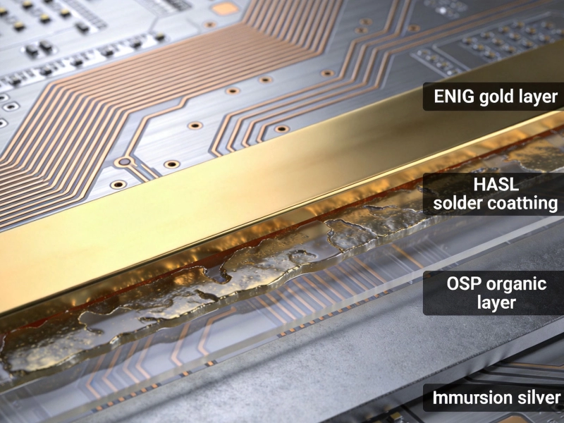
The surface finish protects exposed copper and provides a solderable surface for component assembly. Common options include:
Building boards with multiple copper layers requires careful lamination. The process involves:
Working with experienced manufacturers who understand material behavior is crucial for multi-layer quality.
Standards exist to ensure consistent quality, define acceptable criteria, and provide common language between designers, manufacturers, and customers. Understanding these standards helps you specify requirements accurately and evaluate quotes intelligently.
IPC (Association Connecting Electronics Industries) is the primary standards development organization for the electronics industry. Their standards are used globally and referenced in most professional PCB procurement documents.
The definitive visual inspection standard. Defines what constitutes an acceptable board versus one that should be rejected. Includes acceptance criteria organized by defect type: conductor defects, dielectric defects, holes, and documentation requirements.
Qualification and performance specification for rigid boards. Defines minimum requirements for materials, design, construction, and testing. Covers everything from minimum conductor width to plating requirements.
Similar to Ipc-6012 but specifically addresses Flexible Circuit Materials, Bend Radius requirements, and dynamic flexing applications.
The foundation design document covering all PCB types. Provides design guidelines, Material Selection criteria, and electrical/thermal considerations.
IPC defines three classes of board quality based on the product's service environment. Specifying the correct class prevents over-paying for unnecessary quality or accepting boards unsuitable for your application.
| Class | Name | Application Examples | Key Requirements |
|---|---|---|---|
| Class 1 | General Electronic Products | Toys, basic consumer gadgets, non-critical appliances | Functional requirement, cosmetic defects acceptable |
| Class 2 | Dedicated Service Products | Computers, communications equipment, industrial controllers | Continuous service and extended life, cosmetic defects minimized |
| Class 3 | High Performance/Harsh Environment | Medical devices, aerospace, military, automotive safety systems | Requires continued performance on demand, zero cosmetic defects |
Always specify the appropriate IPC class on your fabrication drawings and purchase orders. A Class 3 board may cost 30-50% more than a Class 1 equivalent, so don't over-specify unless your application truly requires it. Conversely, using Class 1 boards in Class 3 applications risks field failures and potential liability.
Modern Pcb Manufacturing must comply with various environmental regulations:
Understanding fabrication methods and standards enables better design decisions. Here are practical DFM guidelines to improve your PCB designs:
| Specification | Standard | Advanced | HDI |
|---|---|---|---|
| Minimum trace width | 0.15mm | 0.1mm | 0.05mm |
| Minimum trace spacing | 0.15mm | 0.1mm | 0.05mm |
| Minimum via diameter | 0.3mm | 0.2mm | 0.1mm (laser) |
| Annular ring | 0.2mm | 0.15mm | 0.1mm |
| Board thickness tolerance | ±10% | ±5% | ±3% |
For multi-layer boards, maintaining copper balance prevents warpage. When one side has significantly more copper than the other, differential stress causes the board to bend. Solutions include:
Clear fabrication documentation prevents misunderstandings and errors. Always provide:
Selecting the right manufacturer impacts quality, cost, and delivery timeline. Consider these factors:
Understanding PCB fabrication fundamentals empowers you to make better design decisions and communicate more effectively with manufacturers. Whether you're building your first prototype or sourcing thousands of production units, this knowledge serves as your foundation.
Standard FR-4 has a Glass Transition Temperature (Tg) around 130-140°C, while high-Tg variants reach 150-180°C. Higher Tg materials maintain their mechanical properties better during lead-free assembly processes, which expose boards to higher peak temperatures. For RoHS-compliant products with complex assembly, high-Tg is often recommended.
Consider specialty materials when dealing with high frequencies (above 1GHz), high operating temperatures, high power dissipation, or demanding mechanical requirements. If your design specifies Controlled Impedance, analyze whether FR-4's dielectric constant consistency meets your tolerance requirements. Your manufacturer can recommend appropriate materials based on your design parameters.
Class 2 boards are intended for products that require extended continuous service without interruption. This includes most commercial electronics like computers, phones, and industrial equipment. Class 2 allows some cosmetic defects that don't affect functionality but is stricter than Class 1 regarding conductor integrity, hole quality, and documentation.
RoHS regulations restrict lead in most electronics sold in the EU and many other countries. Lead-free finishes (ENIG, HASL LF, OSP) are necessary for compliance. Each has trade-offs: ENIG is flat and reliable but costs more, OSP is economical but has limited shelf life, and lead-free HASL can be uneven for fine-pitch components.
This varies by manufacturer. Many offer low-MOQ programs for prototypes starting at 5-10 boards, while production runs typically start at 100-500 units. Panel utilization affects economics—a manufacturer might quote minimum panel quantity rather than individual boards. Consider your needs: prototypes benefit from small quantities, while production orders reduce per-unit cost significantly.
Industrial Pcb fabrication is a sophisticated process combining materials science, precision engineering, and rigorous quality standards. Understanding the fundamentals—the why behind material choices, the how of fabrication methods, and the what of industry standards—transforms you from someone who specifies boards into someone who truly understands them.
The materials you choose determine your board's electrical and mechanical character. The manufacturing methods you align with affect what you can design and at what cost. The standards you reference ensure clear communication and appropriate quality levels.
Whether you're an engineer designing your first board or a procurement specialist evaluating quotes, this foundation serves you well. The electronics industry continues evolving with new materials, finer geometries, and tighter tolerances, but these core principles remain constant. Master the fundamentals, and you'll navigate the complexities of PCB fabrication with confidence.
Precision Engineering: Tolerances in High-End Industrial PCB FabricationSeptember/03/2026
The Role of Laser Drilling in High-Precision Industrial PCB FabricationOctober/15/2026
Predicting Lifespan: Accelerated Life Testing for Industrial PCB ReliabilityAugust/03/2026
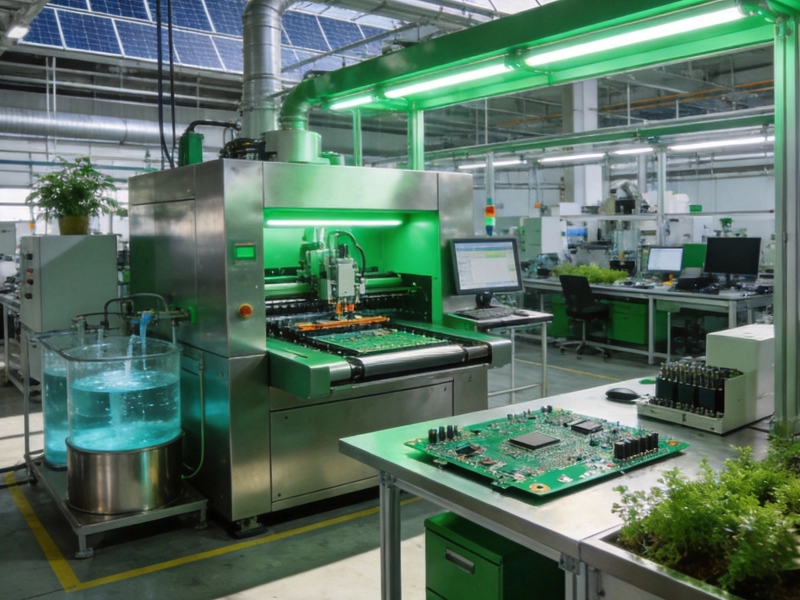
Eco-Friendly Practices in Modern Industrial PCB FabricationSeptember/20/2026
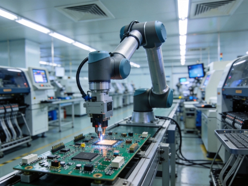
How to Choose the Right Manufacturer for Industrial PCB FabricationJune/29/2026
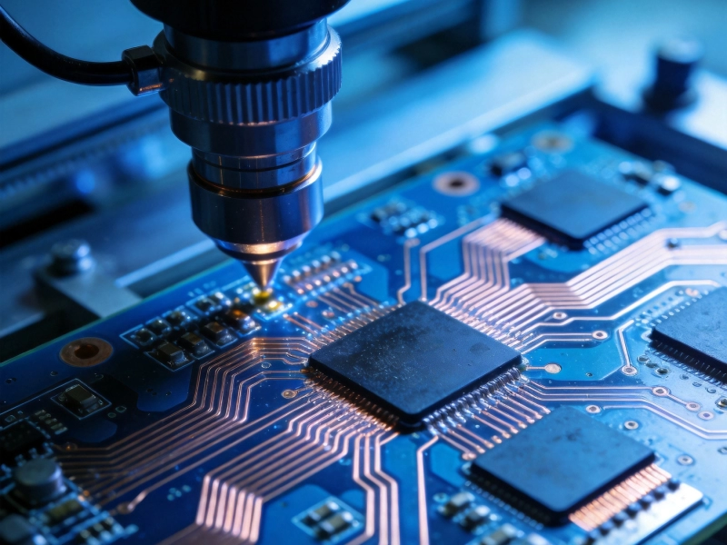
Overcoming Common Defects in Industrial PCB FabricationAugust/03/2026
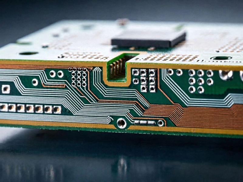
Advanced Techniques in Multi-Layer Industrial PCB FabricationJune/03/2026
The Impact of Surface Finishes on Industrial PCB Fabrication QualityJuly/16/2026