

The rollout of 5G networks across industrial environments has created unprecedented demand for high-frequency PCBs that can reliably operate at frequencies ranging from sub-6 GHz to mmWave bands above 24 GHz. Unlike conventional digital boards where signal integrity is a concern only at the board edge, high-frequency designs require careful consideration of every material choice, layer structure, and manufacturing parameter. Engineers working on industrial IoT applications must balance RF performance requirements against cost, producibility, and long-term reliability in harsh operating conditions.
This guide walks through the critical design decisions that determine success or failure in high-frequency PCB projects for 5G and IoT deployments. From substrate selection to impedance control and Thermal Management, each aspect demands attention that conventional Pcb Design simply does not require.

Industrial 5G applications span a wide frequency spectrum, and understanding where your design must operate directly influences material and stack-up choices. The 3GPP standard defines multiple frequency ranges, with sub-6 GHz deployments (FR1, 410 MHz to 7.125 GHz) representing the most common industrial implementation today, while FR2 mmWave deployments (24.25 to 52.6 GHz) target specialized applications requiring ultra-low latency and high data throughput.
IoT sensor networks operating within industrial facilities often utilize frequencies between 433 MHz and 5.8 GHz, depending on regional regulations and specific use cases. Smart manufacturing equipment, automated guided vehicles, and asset tracking systems each have distinct frequency and bandwidth requirements that drive Pcb Design parameters.
The fundamental challenge is that as signal frequencies increase, traditional Pcb Materials begin exhibiting unwanted dielectric losses, signal dispersion, and impedance variations that degrade communication performance. At 28 GHz and above, even small inconsistencies in trace geometry or substrate properties can result in significant signal attenuation and reflection problems.
The two primary material properties that govern high-frequency Pcb Performance are the dielectric constant (Dk, also called relative permittivity) and the loss tangent (Df). The dielectric constant determines signal propagation velocity and influences trace impedance calculations, while loss tangent quantifies how much signal energy converts to heat during transmission.
Standard FR-4 epoxy glass laminate, the most common Pcb Substrate, exhibits a Dk of approximately 4.2 to 4.5 with loss tangent values between 0.02 and 0.035 at 1 GHz. While acceptable for digital signals up to several hundred megahertz, FR-4 becomes increasingly problematic above 5 GHz due to excessive signal loss and Dk variation across the board. At 28 GHz, FR-4 losses can exceed 3 dB per inch, effectively making it unsuitable for most 5G applications without extremely short trace lengths.
High-frequency laminate materials offer significantly better performance through specialized resin systems and filler compositions. Common options include:
Industrial facilities frequently subject electronic equipment to elevated temperatures, thermal cycling, and humidity variations. High-frequency Pcb Materials must maintain consistent electrical properties across the expected operating temperature range, typically -40°C to +85°C for industrial grade equipment.
The thermal coefficient of dielectric constant (TCDk) measures how much the material's Dk changes with temperature. Materials with low TCDk values provide more stable impedance over temperature, which proves critical for maintaining RF link budgets in outdoor or unconditioned industrial environments. Most high-performance laminates specify TCDk values below 50 ppm/°C, compared to 100-150 ppm/°C for standard FR-4.
Achieving optimal high-frequency Pcb Performance requires thoughtful stack-up design that balances signal routing needs, impedance control requirements, and manufacturing constraints. A typical high-frequency board serving industrial 5G applications might employ a four to six layer configuration, with dedicated reference planes and carefully controlled dielectrics.
The most critical layer is the prepreg immediately adjacent to the signal layer, as this dielectric determines the characteristic impedance of transmission lines. Designers should specify this layer by material type, thickness, and resin content rather than relying on generic stack-up tables. Thickness tolerances of ±10% can produce impedance variations exceeding ±5%, which translates to unacceptable return loss at mmWave frequencies.
Ground reference planes must be continuous and unbroken beneath high-frequency signal traces. Any slots, gaps, or via anti-pads that interrupt the return current path create impedance discontinuities and increase electromagnetic radiation. When crossing between reference planes is unavoidable, stitching vias placed within one-quarter wavelength of the signal path maintain impedance continuity.
High-frequency signal integrity depends on maintaining precise characteristic impedance throughout the signal path. For 5G applications, target impedances of 50 ohms for single-ended signals and 100 ohms differential for high-speed digital interfaces are standard, but tolerances must be tighter than conventional boards.
Industry guidelines typically specify ±10% impedance tolerance for standard digital boards, but mmWave designs may require ±5% or tighter. Achieving this level of control requires consideration of trace width manufacturing tolerances, copper roughness effects, and Solder Mask influence on effective dielectric constant.
Microstrip and stripline are the two primary transmission line topologies used in high-frequency PCB design. Microstrip traces run on outer layers with a reference plane below, offering easier access for testing and modification but greater sensitivity to external fields and Solder Mask variation. Stripline traces reside between two reference planes, providing superior shielding and more predictable impedance but requiring blind or buried vias for signal access.
At high frequencies, current concentrates near the conductor surface rather than distributing evenly through the copper cross-section. This skin effect increases effective resistance and signal attenuation. At 10 GHz, the skin depth in standard copper is approximately 0.66 micrometers, meaning most current flows within the outermost micron of the trace.
Copper surface roughness significantly impacts insertion loss at high frequencies. Standard electrodeposited (ED) copper with roughness of 1-3 micrometers RMS can add 20-30% to total conductor losses at 28 GHz compared to smooth rolled copper. High-frequency PCB manufacturers offer "very low profile" (VLP) or "reverse treated" copper with roughness below 0.5 micrometers for critical applications.
Designers should specify smooth copper for high-frequency signal layers, even though it costs more than standard ED copper. The insertion loss reduction typically provides better RF performance than the additional expense, particularly for long trace runs or high-power transmit paths.
Vias present significant challenges in high-frequency PCB design due to impedance discontinuities they create. Through-hole vias with unsoldered barrels act as transmission line stubs that resonate at specific frequencies, creating severe signal distortion. Designers must carefully consider via treatment for every signal layer transition.
Back-drilling removes unused portion of through-hole barrels beyond the signal layer, eliminating stub resonance effects. This technique works well for frequencies up to approximately 15 GHz but becomes less effective at mmWave frequencies where even minimal stubs cause problems. For 28 GHz and above, blind and buried vias or landless via structures provide the best performance.
Via-in-pad technology, where component leads attach directly over via barrels, offers excellent thermal and electrical performance but requires plated-over via processing. Without proper design attention, capture pad anti-pads can disturb reference plane continuity and create impedance mismatches that degrade signal quality.
High-frequency operation generates heat through both conductor losses in transmission lines and dissipation in active RF components. Industrial IoT equipment often operates in environments with limited cooling, requiring designers to address Thermal Management proactively rather than reactively.
Thermal Vias provide primary heat conduction path from hot components to internal or bottom-side ground planes. Thermal via arrays should place vias within 1 mm of heat-generating components, using via diameters of 0.3 to 0.5 mm with 1 to 1.5 mm pitch for effective heat transfer. Thermal pad designs under QFN, BGA, or other leadless packages require adequate via coverage to prevent localized overheating.
Metal-core PCBs using aluminum or copper substrates offer superior thermal conductivity compared to standard dielectrics, but introduce new design constraints. The coefficient of thermal expansion mismatch between metal core and high-frequency laminate can cause delamination during thermal cycling. Careful material selection and adhesive layer design mitigate these risks for industrial applications requiring wide temperature operation.
High-frequency Pcb Manufacturing demands tighter process controls than standard boards. Trace width tolerances of ±0.5 mil (compared to ±1 mil typical) may be necessary to achieve ±5% impedance control at mmWave frequencies. Etch factor, the ratio of trace width at base versus top, affects effective impedance and should be characterized for the specific fabricator's process.
Laminate thickness control directly influences dielectric thickness and thus impedance. High-frequency boards often specify dielectric tolerance of ±5% or tighter, which most standard fabricators cannot guarantee. Working with manufacturers experienced in RF and microwave PCBs becomes essential for designs operating above 10 GHz.
Surface finish influences both solderability and high-frequency performance. ENIG (electroless nickel immersion gold) provides excellent shelf life and flatness but adds approximately 5 micrometers of nickel and 0.05 to 0.1 micrometers of gold over copper traces. At high frequencies, nickel's magnetic properties and skin effect can increase conductor losses.
For the most demanding mmWave applications, designers may specify immersion silver or OSP (organic solderability preservative) finishes that add minimal conductive material. These finishes require careful handling and processing but minimize RF losses. HASL (hot air solder level) finishes introduce significant topography that disrupts microstrip impedance and should be avoided for high-frequency signal layers.
Prototype validation for high-frequency PCBs requires measurement capabilities beyond standard digital board testing. Time-domain reflectometry (TDR) characterizes impedance discontinuities along transmission paths, identifying problems before full RF testing. Vector network analyzers (VNAs) measure S-parameters that quantify insertion loss, return loss, and impedance across frequency.
Designers should include test coupons on production panels that undergo the same processing as production boards. These coupons, with precisely characterized trace structures, enable correlation between simulated and measured performance. Any significant discrepancies point to material property variations, process effects, or modeling assumptions that require correction before production release.
Environmental testing under temperature, humidity, and vibration conditions verifies that high-frequency performance remains stable throughout product lifetime. Accelerated life testing protocols developed for aerospace and automotive RF assemblies provide reference methodologies for industrial IoT equipment qualification.
Designing high-frequency PCBs for industrial 5G and IoT applications demands attention to material properties, stack-up geometry, and manufacturing processes that conventional PCB design overlooks. Success requires selecting appropriate high-frequency laminates with low loss tangent and stable dielectric constant, implementing controlled impedance structures with tight tolerances, and working with fabricators capable of meeting the required manufacturing precision.
Thermal management considerations must be integrated early in the design process rather than addressed as afterthoughts. Via treatment strategies, copper profile selection, and surface finish choices all influence final RF performance and must align with the target operating frequency and environmental conditions.
By understanding these fundamentals and applying systematic validation procedures, engineers can develop high-frequency PCBs that meet the demanding requirements of industrial 5G and IoT deployments while balancing performance, cost, and manufacturability.
Substrate thickness depends on the required impedance and trace geometry. For 50-ohm microstrip on common high-frequency laminates, substrate thicknesses of 5 to 10 mils (0.127 to 0.254 mm) provide practical trace widths. Thinner substrates enable tighter bends but increase sensitivity to manufacturing variations.
FR-4 can work for sub-6 GHz designs with short trace lengths, but dielectric losses limit maximum path lengths. For designs exceeding several centimeters at frequencies above 3 GHz, high-frequency laminates typically provide better overall performance and more consistent impedance control.
High-frequency PCB costs typically run 2 to 5 times higher than equivalent standard boards, depending on material selection, tolerance requirements, and special processing needs. PTFE materials command premium pricing due to processing complexity, while hydrocarbon ceramics offer better cost-positioning for many industrial applications.
Most 5G applications specify ±10% impedance tolerance, achievable with careful design and standard high-quality fabrication. mmWave designs operating above 24 GHz often require ±5% or tighter, necessitating premium materials and enhanced process controls.
Microstrip suits applications where trace access for testing matters, moderate frequency ranges (below 20 GHz), and where external shielding through enclosure design is acceptable. Stripline provides better isolation and impedance predictability for frequencies above 20 GHz or where electromagnetic radiation must be minimized.
Design Guidelines for Durable Flex PCB Solutions in Dynamic ApplicationsJuly/10/2026
Heavy Copper PCBs: The Solution for High-Current Industrial ApplicationsJune/18/2026

Tailored Industrial PCB Solutions for Medical Device ManufacturersJune/12/2026
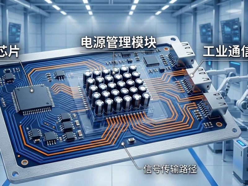
Unlocking Performance with High-Layer Count Industrial PCB SolutionsJune/15/2026

End-to-End Industrial PCB Solutions: From Design to DeliveryJuly/08/2026
Why Choose Rigid-Flex PCB Solutions for Complex Industrial Assemblies?June/17/2026
Custom Industrial PCB Solutions for the Automotive SectorMay/27/2026
An Introduction to HDI Technology for Compact Industrial ElectronicsJune/16/2026