Open Nav


Flexible printed circuit boards have transformed electronics design by enabling connections in three-dimensional space, reducing weight, and allowing products to conform to complex shapes. However, designing flexible PCBs for dynamic applications—where the flex circuit will bend, twist, or flex repeatedly during product use—requires careful attention to design details that directly affect durability and reliability. Unlike rigid boards that are stationary once assembled, Flexible Circuits in dynamic applications experience mechanical stress that can lead to conductor cracking, delamination, or complete failure if not properly designed. This comprehensive guide provides essential design guidelines for creating flexible PCBs that maintain electrical and mechanical integrity through thousands or millions of flex cycles.

Before diving into specific design guidelines, it's essential to understand the different types of dynamic flex applications and their unique requirements. Not all Flexible Circuits experience the same types or degrees of mechanical stress.
Dynamic flex applications typically fall into two categories based on the type of mechanical motion. Bending applications involve the circuit folding back and forth along a single axis, similar to a door hinge. Common examples include laptop hinges, folding phone mechanisms, and robotic joint connections. These applications typically experience thousands to millions of bend cycles over the product lifetime.
Twisting applications involve rotation around the circuit's longitudinal axis, as seen in rotating camera modules, antenna deployment mechanisms, and some medical catheters. Twisting creates different stress patterns in the conductors and requires specific design considerations.
Some applications combine both bending and twisting, creating the most demanding mechanical requirements. Wearable devices, for example, may experience complex multidirectional flexing as the device conforms to body movement.
The expected number of flex cycles dramatically influences design choices. Static flex applications that bend once during installation and remain fixed can use simpler designs than dynamic flex applications that must survive repeated cycling. Cycle requirements typically fall into these ranges:
Dynamic flex applications often operate in challenging environments that affect durability. Temperature extremes affect material properties and thermal expansion differences. Humidity can cause material swelling and affect adhesion. Chemical exposure from cleaning agents, bodily fluids, or industrial chemicals can degrade materials. Design must account for these environmental factors in addition to mechanical stress.
The foundation of durable flexible Pcb Design lies in appropriate material selection. Different materials offer varying combinations of flexibility, durability, thermal stability, and cost.
Polyimide (PI) is the industry standard for flexible PCBs due to its excellent combination of mechanical properties and thermal stability. Polyimide can withstand temperatures from -269°C to +400°C, maintains mechanical properties after thousands of flex cycles, and offers excellent dimensional stability. While more expensive than alternatives, polyimide is the preferred choice for demanding dynamic applications.
Polyester (PET) provides a lower-cost option for less demanding applications. However, polyester has significantly lower thermal resistance (typically limited to +105°C) and inferior mechanical performance under repeated flexing. Polyester is suitable for low-cost, low-cycle applications but should not be used in demanding dynamic flex scenarios.
Polyethylene naphthalate (PEN) offers intermediate performance between polyester and polyimide, with better thermal resistance and mechanical properties than polyester but at a lower cost than polyimide. PEN can be appropriate for moderate dynamic applications where polyimide cost cannot be justified.
Rolled annealed copper is the standard conductor material for dynamic flex circuits due to its superior flexibility compared to electro-deposited copper. The rolling process aligns the copper grain structure along the rolling direction, providing significantly better performance under repeated bending. Standard copper foil thicknesses for dynamic flex range from 1/2 oz (17.5 μm) to 2 oz (70 μm).
For extreme dynamic applications requiring thousands of flex cycles, consider using ultra-thin copper foils. Thinner copper has lower bending stiffness and experiences less stress during flexing. However, thinner copper also has higher resistance and may require wider traces for current-carrying capacity.
Adhesiveless constructions are increasingly preferred for dynamic flex applications because they eliminate the adhesive layer that can become a point of failure during flexing. However, adhesiveless materials are more expensive and may have different processing requirements.
When adhesive is necessary, acrylic adhesives generally provide better flexibility than epoxy adhesives for dynamic applications. The adhesive thickness should be minimized while still providing adequate bonding and dielectric strength.
Coverlay materials protect the conductors and provide additional mechanical strength. Polyimide coverlay is the most common choice, though liquid photoimageable coverlay (LPI) can provide thinner profiles and better coverage in complex geometries. Coverlay thickness typically ranges from 1 mil (25 μm) to 2 mils (50 μm).
Perhaps the most critical design parameter for dynamic flex circuits is the minimum bend radius—the smallest radius the circuit will experience during operation. Bending tighter than the minimum bend radius dramatically increases conductor stress and accelerates failure.
The minimum bend radius depends on the overall circuit thickness and construction type. For single-sided flex circuits, a common rule is that the minimum bend radius should be at least 6-10 times the overall circuit thickness. For double-sided circuits, increase this to 10-15 times the thickness.
More precise calculations consider the specific construction. For a flexible circuit with overall thickness T, the minimum dynamic bend radius should be approximately 10×T for occasional flexing (10-100 cycles), 15×T for regular flexing (100-1,000 cycles), and 20×T for frequent flexing (1,000+ cycles).
Placing the conductors at or near the neutral bend axis—the axis within the circuit that experiences neither compression nor tension during bending—is crucial for durability. The neutral axis is typically located at the center of the circuit thickness.
Symmetrical constructions with conductors on both sides of the dielectric center help balance stresses. If conductors must be placed away from the neutral axis, design measures such as wider traces, rounded corners, and stress-relief patterns become even more important.
Design for consistent curvature across the bent section. Abrupt changes in curvature create stress concentrations that lead to premature failure. When the bend radius changes, use gradual transitions rather than sharp changes in curvature.
Avoid placing stiff components or connectors directly at the bend area. These features act as hard spots that concentrate stress. Provide at least 3-5 times the bend radius of straight, unstiffened conductor on either side of components near bend areas.
How conductors are routed through bend areas significantly affects durability. Strategic conductor design reduces stress concentrations and improves cycle life.
Wider traces are more durable than narrow traces under repeated flexing because they distribute stress over a larger area and provide more material to withstand mechanical stress. While wider traces consume more space, they significantly improve reliability in dynamic applications.
When space constraints force the use of narrow traces, maintain consistent width through bend areas. Avoid varying trace width in bend sections as width changes create stress concentrations. Ensure adequate spacing between parallel traces in bend areas—spacing should be at least 2-3 times the trace width to prevent adjacent trace failures from propagating.
Use curved corners rather than sharp 90-degree angles in bend areas. A minimum corner radius of 2-3 times the trace width helps distribute stress more evenly. For high-cycle applications, consider corner radii of 5-10 times trace width.
If sharp corners are unavoidable, add stress-relief features such as rounded teardrops or widened sections at corners. These features reduce the stress concentration that would otherwise occur at sharp inside corners.
When routing multiple parallel traces through a bend area, stagger them rather than aligning them in a straight line perpendicular to the bend. Staggering prevents stress concentrations from aligning and propagating between adjacent traces. A common practice is to offset parallel traces by 1-2 trace widths.
For high-density parallel traces in bend areas, consider adding dummy traces between signal traces. These non-functional traces provide additional mechanical support and help distribute stress more evenly across the array.
Vias represent points of mechanical discontinuity in flexible circuits and should be minimized in bend areas. When vias are necessary near bend zones, design them with careful attention to mechanical stress.
Use teardrop-shaped pads around vias to distribute stress from the via into the surrounding copper. Ensure adequate copper area around vias to provide mechanical support. Avoid placing vias directly in the neutral bend axis if possible—vias on the outside of a bend experience less tension than those on the inside.
The overall construction of the flexible circuit affects its mechanical performance. Careful layer stack design can significantly improve durability.
Maintain symmetry in the layer stack about the neutral axis. Asymmetric constructions create uneven stress distribution during flexing, leading to warpage and differential stress between layers. Symmetrical constructions with balanced copper area on both sides of the dielectric provide the most predictable mechanical performance.
Distribute copper weight evenly across the layer stack. Concentrating heavy copper on one side creates imbalance and increases stress on that side during flexing. If different copper weights are necessary, place heavier copper layers closer to the neutral axis to minimize the bending moment created during flexing.
Thinner dielectric materials generally improve flexibility by reducing overall circuit thickness and moving conductors closer to the neutral axis. However, thinner dielectrics may have reduced mechanical strength and lower dielectric strength. Balance flexibility requirements with mechanical robustness and electrical isolation needs.
When possible, use thinner dielectrics in bend areas and thicker dielectrics in flat areas that do not flex. This approach optimizes both flexibility and mechanical strength where each is needed.
Even with proper basic design, additional stress relief and reinforcement techniques can dramatically improve durability in demanding applications.
Stiffeners (typically polyimide or FR-4) reinforce specific areas of the flex circuit to prevent unwanted bending and protect components. Place stiffeners strategically to direct bending to specific areas while protecting other sections.
Avoid placing stiffeners directly at bend points. Instead, terminate stiffeners 1-2 times the bend radius away from the bend area. This gradual transition prevents stress concentrations at stiffener boundaries.
Design strain relief features where the flex circuit transitions to rigid areas or connectors. These features reduce stress at mechanical discontinuities. Common strain relief techniques include:
Design secure anchor points where the flex circuit attaches to rigid structures or components. Loose or poorly anchored flex circuits experience excessive movement and stress. Use appropriate mechanical fasteners, adhesives, or potting materials to create stable anchor points that prevent unwanted movement while still allowing designed flexing.
Design decisions affect manufacturability, and manufacturing processes influence final product durability. Understanding these interactions helps create designs that are both reliable and manufacturable.
Ensure design choices are compatible with available manufacturing processes. Some features that improve theoretical durability may be impractical to manufacture reliably. Consult with fabricators early in the design process to understand process capabilities and limitations.
Flexible materials have different dimensional stability characteristics than rigid materials. Polyimide, for example, has different thermal expansion characteristics in the machine and transverse directions. Design tolerances must account for these material properties and expected manufacturing variations.
Establish appropriate inspection and testing procedures for dynamic flex circuits. Visual inspection should check for conductor damage, coverlay issues, and dimensional accuracy. Electrical testing should verify continuity and insulation resistance. For critical applications, consider implementing flex cycle testing as part of quality assurance.
Comprehensive testing and validation are essential to ensure flexible circuits will perform reliably in their intended applications. Testing should simulate actual use conditions to validate design assumptions.
Perform accelerated flex cycle testing on representative samples. Test conditions should match or exceed actual use conditions including bend radius, flex frequency, and environmental factors. Monitor electrical continuity and mechanical integrity throughout testing.
Test to multiple times the expected design life. If the product should survive 100,000 cycles, test to 300,000-500,000 cycles to provide adequate margin. Analyze failure modes from any samples that fail during testing and implement design improvements.
Combine flex cycle testing with environmental stress testing. Temperature cycling, humidity exposure, and chemical exposure during flex cycles reveal combined stress effects that might not appear from testing each stress individually.
Whenever possible, test flex circuits in actual product assemblies or realistic mock-ups. Testing bare flex circuits provides useful data, but final validation should occur in the context of actual product mounting and use conditions.
Understanding common failure modes helps design flex circuits that avoid these pitfalls. Most failures result from preventable design oversights rather than material limitations.
Conductor cracking is the most common failure mode in dynamic flex circuits. Cracks typically initiate at stress concentrations such as sharp corners, vias, or trace width changes. Prevention involves rounded corners, consistent trace widths, stress-relief patterns, and ensuring conductors are near the neutral bend axis.
Delamination occurs when layers separate during flexing. This typically results from inadequate adhesive bonding, thermal expansion mismatch, or stress concentrations at layer boundaries. Prevention includes appropriate material selection, proper adhesive application, symmetrical construction, and gradual stiffness transitions.
Coverlay materials can crack under repeated flexing, particularly at corners or stress points. Thinner, more flexible coverlay materials are less prone to cracking. Coverlay should be placed carefully to avoid creating hard spots in bend areas. Liquid coverlay can provide better coverage and flexibility than film coverlay in complex geometries.
Vias can fail due to mechanical stress, plating defects, or thermal cycling. Proper via design with adequate plating thickness, teardrop pads, and avoidance of bend areas reduces via failure risk. Consider using buried vias in bend areas when possible to move the stress point away from the neutral axis.
Applying these comprehensive guidelines requires balancing multiple design considerations. The following best practices provide a practical framework for durable flexible Pcb Design.
Involve fabricators, material suppliers, and application experts early in the design process. Their expertise can prevent design choices that look good on paper but are impractical or unreliable in practice.
Use finite element analysis (FEA) or other simulation tools to analyze stress distribution in bend areas. Simulation can identify potential problem areas before prototypes are built, saving time and cost. Validate simulation results with physical testing.
Build adequate design margins into flex circuits. The cost of over-designing flexibility is usually minimal compared to the cost of field failures. Design for more flex cycles and tighter bend radii than the minimum specified requirements.
Clearly document flex requirements including bend radius, flex cycles, and environmental conditions. Ensure all stakeholders understand these requirements and their design implications. Good communication prevents misunderstandings that lead to inadequate designs.
Plan for iterative design cycles. The first design iteration may reveal issues that require refinement. Build testing into the development schedule rather than treating it as a final validation step. Learn from failures and continuously improve the design.
Designing durable flexible PCBs for dynamic applications requires attention to material properties, mechanical geometry, manufacturing processes, and testing requirements. While flexible circuits present additional design challenges compared to rigid boards, following established guidelines and best practices enables creation of reliable solutions that survive thousands or millions of flex cycles in demanding applications.
The key principles include selecting appropriate materials for the application requirements, maintaining adequate bend radii with conductors near the neutral axis, using rounded corners and stress-relief features, distributing stresses evenly through symmetrical constructions, and validating designs through comprehensive testing.
As electronic devices continue to incorporate more flexible and conformal designs, the demand for reliable dynamic flex circuits will continue to grow. Designers who master these guidelines will be well-positioned to create innovative products that leverage the unique capabilities of flexible circuit technology while maintaining the reliability that users expect.
Success in flexible PCB design comes from understanding the fundamental mechanical behavior of flexible materials and applying this understanding through careful, detail-oriented design practice. The difference between a flexible circuit that fails after a few hundred cycles and one that lasts through millions of cycles often comes down to attention to these seemingly small but critical design details.
The minimum bend radius depends on circuit thickness and construction. As a general guideline, use 10× overall thickness for occasional flexing (10-100 cycles), 15× for regular flexing (100-1,000 cycles), and 20× for frequent flexing (1,000+ cycles). More precise calculations consider the specific layer stack and material properties.
Flex cycle life varies dramatically based on design and construction. Well-designed flexible circuits can survive 100,000 to 1,000,000+ cycles when properly designed with adequate bend radii, appropriate materials, and stress-relief features. Poorly designed circuits may fail after only a few hundred cycles.
Standard FR-4 is not suitable for dynamic flex applications because it lacks the flexibility to withstand repeated bending without cracking. Polyimide is the industry standard for flexible PCBs due to its excellent flexibility and thermal stability. Polyester and PEN may be used for less demanding applications but have lower performance limits.
Generally, avoid placing components directly on flexible sections that will bend during use. Components create stiff spots that concentrate stress. Place components on rigid sections or stiffened areas of the flex circuit. If components must be on flexible sections, design with very generous bend radii and extensive stress relief.
Testing should simulate actual use conditions including bend radius, flex frequency, and environmental factors. Accelerated flex cycle testing is essential, typically testing to 3-5 times the expected design life. Combine flex testing with environmental testing including temperature cycling and humidity exposure. Validate with real-world assembly testing whenever possible.
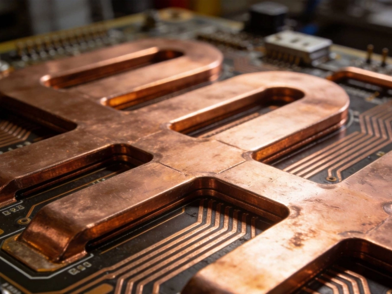
Heavy Copper PCBs: The Solution for High-Current Industrial ApplicationsJune/18/2026

Unlocking Performance with High-Layer Count Industrial PCB SolutionsJune/15/2026

Tailored Industrial PCB Solutions for Medical Device ManufacturersJune/12/2026
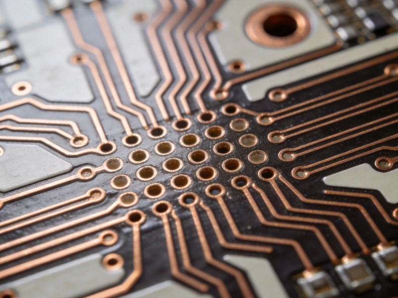
An Introduction to HDI Technology for Compact Industrial ElectronicsJune/16/2026
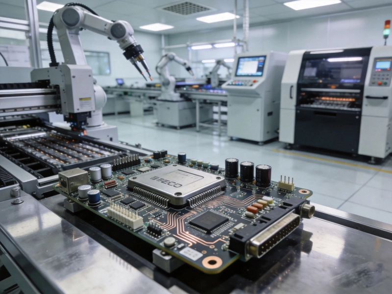
Custom Industrial PCB Solutions for the Automotive SectorMay/27/2026
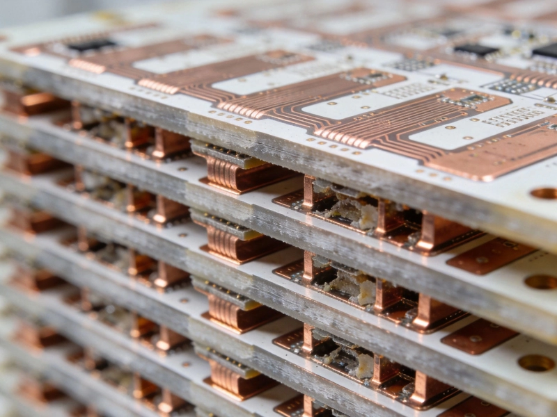
Manufacturing Challenges in 20+ Layer Industrial PCB SolutionsJuly/09/2026

Designing High-Frequency PCBs for Industrial 5G and IoT ApplicationsJune/26/2026
End-to-End Industrial PCB Solutions: From Design to DeliveryJuly/08/2026