Open Nav


Design for Manufacturability represents one of the most critical yet frequently overlooked aspects of Industrial Pcb development. Despite advances in manufacturing technology and design automation, costly mistakes continue to plague PCB projects across industries, resulting in production delays, elevated costs, quality compromises, and in severe cases, complete project failures. The difference between a successful product launch and a costly redesign often hinges on decisions made during the earliest design phases—before any physical prototypes exist, before manufacturing specifications are finalized, and before the consequences of design choices become apparent.
Industry data consistently reveals that the majority of Pcb Manufacturing problems originate from design-stage oversights rather than manufacturing process failures. When design teams fail to consider manufacturability requirements, they inadvertently create boards that are difficult to produce, require special processing, demand expensive tooling, or simply cannot be manufactured within acceptable quality parameters. These design-induced problems cascade through production, multiplying costs at each stage and often surfacing only when manufacturing attempts reveal incompatibilities that force expensive rework or complete redesign.
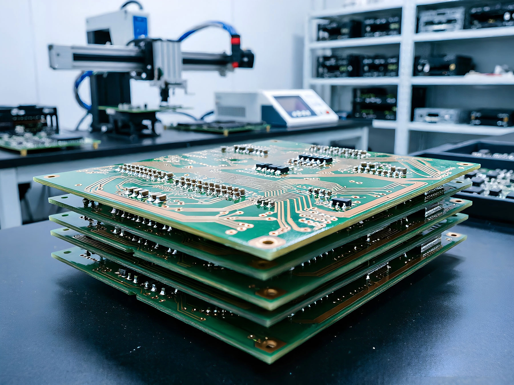
PCB DFM encompasses the practices, analysis methods, and design guidelines that ensure printed circuit boards can be manufactured efficiently, reliably, and cost-effectively at production volumes. Rather than treating manufacturing as a separate downstream activity, DFM integrates manufacturing considerations throughout the design process, enabling informed decisions that optimize the design for the realities of production processes. This proactive approach prevents problems before they occur, rather than discovering them through expensive trial and error during manufacturing attempts.
The scope of PCB DFM extends across multiple dimensions including design rule verification, process capability analysis, material compatibility assessment, testability planning, and assembly optimization. Effective DFM requires collaboration between design engineers who understand application requirements and manufacturing engineers who understand process capabilities. This interdisciplinary approach ensures that designs are not merely technically sound but also aligned with the practical realities of how boards will actually be fabricated, assembled, and tested.
Understanding the economic impact of DFM decisions illuminates why proper design-phase consideration delivers such substantial returns. Industry research demonstrates that fixing design errors discovered after manufacturing begins costs an average of ten times more than addressing the same issues during initial design. Errors discovered during production scale-up cost one hundred times more, while field failures trigger costs approaching one thousand times the original design-phase fix cost. These multipliers create compelling economic justification for investing in comprehensive DFM practices that prevent problems rather than reacting to them.
The total cost impact extends far beyond direct rework expenses. Production delays disrupt delivery commitments, strain customer relationships, and may trigger contractual penalties. Expedited shipping for critical components to replace damaged stock adds logistics costs. Engineering resources diverted to problem-solving cannot work on new development. In worst cases, DFM failures create quality escapes that reach customers, triggering recalls, warranty claims, and reputation damage that far exceed the original manufacturing cost impact.
Understanding the most frequently encountered DFM failures provides a foundation for developing effective prevention strategies. These recurring problems have accumulated across countless PCB projects, creating a body of knowledge about what goes wrong and how to prevent it. Each category represents systematic failures that proper DFM processes can effectively address.
Gerber file format errors consistently rank among the most common reasons manufacturing facilities reject design submissions. Problems include using non-standard Gerber formats without embedded aperture tables, missing files in complete design packages, inconsistent coordinate systems between layers, and errors in drill files that specify incorrect hole sizes or plating requirements. These documentation failures prevent CAM systems from properly interpreting design intent, causing manufacturing delays while errors are identified and corrected.
The consequences extend beyond simple file rejections. Incomplete documentation may force manufacturing engineers to make assumptions about design intent, potentially introducing errors that go undetected until later inspection. Improper Gerber format may cause mis-interpretation of features, potentially creating boards that match the erroneous file rather than the intended design. These hidden errors multiply costs through scrap, rework, and in severe cases, customer returns of completed assemblies.
Component footprint mismatches represent one of the most costly DFM failures in volume production. This problem typically occurs when component selections change during design evolution but corresponding PCB footprints fail to update accordingly. The result is a systematic mismatch between component geometry and pad design that prevents proper placement, soldering, or functionality. Boards may appear to assemble correctly but exhibit intermittent connections, stress fractures under Thermal Cycling, or complete functional failures.
The financial impact of footprint mismatches multiplies through production volume. Unlike a single prototype that can be reworked manually, volume production with systematic footprint errors generates exponentially increasing scrap and rework costs. Production lines may need to stop while engineering investigates field failures, incurring massive opportunity costs from disrupted schedules. The root cause—failure to maintain synchronization between component library updates and PCB footprint designs—represents a process deficiency that comprehensive DFM checklist verification would catch before manufacturing begins.
Designs that violate minimum spacing requirements between conductors, pads, and other features create manufacturing problems that may not become apparent until production attempts reveal process capability limitations. While Design Rule Checks can flag spacing violations against absolute minimums, DFM analysis considers realistic manufacturing tolerances that may require more conservative spacing to achieve acceptable yields.
Conductor spacing violations cause various problems depending on the nature of the violation. Insufficient spacing between adjacent traces creates risks of shorts during manufacturing or operation. Inadequate pad-to-pad spacing prevents proper Solder Mask definition, potentially causing bridging during assembly. Inadequate spacing around mounting holes prevents proper routing or creates assembly interference. Each violation type requires specific manufacturing workarounds or redesign to resolve, adding cost and delay to projects.
Designs that fail to account for thermal requirements during operation create reliability problems that may not surface for months or years of field service. Thermal Management DFM encompasses both manufacturing thermal stresses and operational Heat Dissipation. Designs must accommodate the heat generated during soldering processes while providing adequate thermal paths for components during operation.
Thermal-related DFM failures manifest as field reliability problems that damage customer relationships and product reputation. Delamination occurs when boards experience temperatures exceeding material limits during assembly or operation. Vias can fail under Thermal Cycling stress when thermal relief is inadequate. High-power components can overheat when thermal pads, planes, and heat sinks are improperly designed. These reliability failures impose costs far exceeding the original design modifications that could have prevented them.
Comprehensive DFM requires systematic verification procedures that check designs against manufacturing capabilities at multiple stages of completion. These verification procedures should integrate with design workflows, providing feedback early when corrections are inexpensive and late changes are still feasible.
Design Rule Checks (DRC) form the foundation of DFM verification by systematically checking designs against predefined design rules. These automated checks verify spacing, connection integrity, annular ring dimensions, via sizes, trace widths, and countless other parameters against both absolute design rules and manufacturing capability limits. Running comprehensive DRC before design completion catches countless errors that would otherwise reach manufacturing.
Electrical Rule Checks (ERC) complement DRC by verifying electrical connectivity and Signal Integrity. ERC identifies floating nets, unconnected power pins, missing bypass capacitors, and other electrical design issues that affect circuit functionality. While DRC focuses on manufacturability parameters, ERC ensures designs meet functional requirements. Together, these automated verification tools catch the majority of systematic errors before manufacturing review.
Netlist verification ensures that the physical Pcb Layout accurately reflects the schematic design. Netlist comparison between schematic and layout catches errors including missing connections, unintended shorts, swapped pins, and other connectivity problems that may not trigger DRC violations but nonetheless represent design errors. This verification is particularly important for complex designs with dense routing where human review cannot reliably catch all connectivity issues.
Manufacturing netlist verification extends this concept by comparing design netlists against actual board measurements. Electrical testing of manufactured boards generates a defect netlist that identifies opens, shorts, and resistance anomalies. Comparing this manufacturing netlist against the design netlist identifies assembly defects, manufacturing errors, and in some cases, design errors that escaped earlier verification. This closed-loop verification ensures that designs translate correctly into functional assemblies.
Beyond checking designs against arbitrary rules, comprehensive DFM verifies designs against specific manufacturing capabilities. This analysis requires understanding the capabilities of intended manufacturing partners, including their minimum feature sizes, registration accuracy, impedance control tolerances, and material options. Designs optimized for state-of-the-art manufacturing facilities may be unproduceable at vendors with more conservative capabilities.
Design for Test (Dft) analysis ensures that manufactured boards can be properly tested to verify functionality. This includes planning for Test Points, access for probe placement, and Boundary Scan compatibility where applicable. Boards that cannot be adequately tested represent quality risks, as manufacturing defects may escape detection and reach customers. DFM analysis of test requirements ensures that testability is designed in rather than retrofitted after layout is complete.
Effective DFM requires more than automated checking—it demands a comprehensive approach that integrates manufacturing considerations throughout the design process. The following best practices provide a framework for achieving DFM success in industrial applications where reliability, quality, and cost-effectiveness are paramount.
The most effective DFM programs engage manufacturing expertise early in design, before critical decisions become fixed. Design reviews with manufacturing engineering participation at concept and preliminary design phases identify potential manufacturability issues when changes are inexpensive. This early engagement prevents designs from progressing down paths that would create manufacturing difficulties, avoiding costly redesigns later in development.
Early DFM engagement also builds relationships and communication channels between design and manufacturing teams. When manufacturing engineers understand design intent and constraints, they can provide more valuable guidance throughout development. When design engineers understand manufacturing capabilities and limitations, they can make informed tradeoffs that optimize designs for production. This collaborative approach produces better outcomes than adversarial relationships where design and manufacturing operate in isolation.
Standardized design rules that incorporate manufacturing capabilities provide consistent guidance throughout design organizations. Rather than requiring individual engineers to research manufacturing specifications, standardized rules encode collective knowledge about what can and cannot be manufactured reliably. These rules should reflect actual manufacturing partner capabilities, incorporate appropriate safety margins, and update as manufacturing processes evolve.
Component library standardization ensures that footprints, symbols, and 3D models remain consistent across projects and design teams. Standardized libraries incorporate DFM considerations including proper pad geometry, thermal relief, and Solder Mask clearance. Engineers who use standardized libraries automatically implement DFM best practices without requiring deep manufacturing expertise. Library maintenance processes ensure that standards remain current as new components enter the market.
Formal design reviews at defined milestones provide structured opportunities to identify and address DFM issues before they propagate to manufacturing. Review checklists should include specific DFM verification items that go beyond technical correctness to address manufacturability. Review participants should include manufacturing engineering representation that can identify potential production issues based on design characteristics.
Design reviews should examine manufacturing outputs including Gerber files, drill files, and assembly drawings for completeness and correctness. Manufacturing engineers reviewing these outputs can identify issues that automated tools may miss, including ambiguous specifications, inconsistent conventions, or requirements that exceed stated capabilities. This human review layer catches the edge cases and unusual situations where automated DFM may provide false confidence.
Close collaboration with manufacturing partners throughout development ensures that designs align with actual production capabilities and constraints. This collaboration should extend beyond simple design rule specification to include process consultation, capability assessment, and Continuous Improvement based on manufacturing feedback. Partners who understand your application requirements can provide guidance specific to your quality and reliability needs.
Manufacturing partner feedback from production runs provides invaluable information for DFM improvement. Analyzing defect patterns, yield issues, and customer returns identifies design practices that create manufacturing difficulties or quality risks. This feedback loop enables continuous refinement of DFM guidelines and design rules, progressively improving design maturity across product generations.
Different manufacturing processes impose different constraints and opportunities on Pcb Design. Effective DFM tailors verification and optimization to specific production approaches rather than applying generic rules.
Surface mount technology (SMT) imposes specific DFM requirements related to paste application, component placement, and reflow soldering. Stencil design for proper paste volume requires appropriate pad sizing relative to component leads and appropriate aperture geometry for reliable paste release. Component placement requires adequate clearance around parts for vision system access and pick-and-place tooling clearance. Reflow considerations include thermal profile compatibility across components with varying thermal mass.
SMT DFM also addresses component density, routing accessibility for production equipment, and coplanarity requirements for large leadless packages. Boards designed with SMT DFM principles assemble reliably at high yield rates, reducing per-unit costs and quality risks. Designs that ignore SMT manufacturing realities generate costly assembly problems including tombstones, bridging, insufficient solder, and component damage.
Designs incorporating through-hole components require additional DFM considerations for wave soldering, selective soldering, or hand assembly processes. Through-hole DFM addresses lead bend requirements, hole sizing for component leads, annular ring requirements for plated holes, and solder fill requirements for reliable connections. Mixed technology boards with both SMT and through-hole components require careful sequencing to ensure assembly processes do not damage previously assembled components.
Through-hole technology continues important in applications requiring high current capacity, mechanical mounting, or connectors incompatible with surface mounting. DFM for through-hole designs must address the specific capabilities and limitations of applicable assembly processes, whether wave soldering for standard through-hole, selective soldering for mixed technology, or invasive reflow for advanced packages.
High-density interconnect (HDI) designs with Microvias, blind and buried vias, and fine line geometries impose stringent DFM requirements that differ substantially from standard PCB processes. HDI DFM addresses Sequential Lamination constraints, laser drill capabilities, Via-in-pad requirements, and registration tolerances that determine achievable feature densities. Designs must account for the specific HDI manufacturing sequence to ensure that layer builds support required interconnect.
The higher costs and longer cycle times associated with HDI manufacturing make DFM particularly valuable for these designs. Errors discovered during expensive HDI production create significant financial impact. Comprehensive HDI DFM verification before manufacturing submission prevents costly delays and ensures that expensive HDI processes produce functional boards on first attempts.
Establishing effective DFM practices requires systematic implementation that addresses people, processes, and tools. Without adequate attention to all three dimensions, DFM initiatives fall short of their potential impact.
Modern EDA tools provide increasingly sophisticated DFM capabilities that automate verification of design rules, manufacturing capabilities, and design-for-test requirements. Implementing comprehensive DFM tool configurations that reflect actual manufacturing capabilities ensures consistent verification across all designs. Tool configuration management maintains rule sets that evolve with manufacturing partner capabilities and organizational learning.
Advanced DFM tools incorporate process simulation capabilities that predict manufacturing outcomes based on design characteristics. These tools can model paste release, predict defect probabilities, and identify high-risk areas requiring design modification or manufacturing process adjustment. While such simulations require validation against actual production data, they provide valuable guidance for optimizing designs before manufacturing commitment.
DFM effectiveness depends ultimately on the skills and knowledge of the people who perform design and manufacturing engineering functions. Training programs should develop understanding of manufacturing processes, their capabilities and limitations, and the design practices that optimize for producibility. Engineers with strong DFM skills make better design decisions throughout development, not just when formal verification catches problems.
Cross-functional development experiences that rotate engineers between design and manufacturing roles build appreciation for both perspectives. Engineers who understand manufacturing challenges make better design tradeoffs. Manufacturing engineers who understand design requirements provide more valuable guidance. These cross-functional skills improve organization-wide DFM capability beyond what formal procedures alone can achieve.
Measuring DFM effectiveness through appropriate metrics enables Continuous Improvement and accountability. Metrics should track DFM-related issues at various stages including design verification, manufacturing introduction, production, and field performance. Correlating DFM metric trends with design complexity, process changes, and manufacturing partner performance identifies opportunities for improvement.
Continuous improvement processes ensure that DFM practices evolve based on lessons learned from production experience. Root cause analysis of manufacturing issues that trace to design deficiencies informs updates to design rules, verification procedures, and training curricula. This feedback loop progressively raises organizational DFM capability, reducing preventable errors and improving product quality.
Proper PCB DFM transforms from cost center to competitive advantage when organizations recognize its strategic importance. Designs optimized for manufacturing through comprehensive DFM practices achieve higher yields, lower costs, better quality, and faster time-to-market than designs that treat manufacturing as an afterthought. These advantages compound across product generations as organizational DFM capability matures and design teams internalize manufacturing-aware practices.
The investment in DFM capabilities pays returns across multiple dimensions. Direct cost savings from reduced scrap, rework, and redesign multiply through production volumes. Schedule advantages from faster manufacturing introduction translate to market timing benefits. Quality improvements from design-phase error prevention protect brand reputation and customer relationships. These combined benefits make DFM one of the highest-return investments available in PCB development.
Organizations that establish robust DFM programs position themselves advantageously in competitive markets where efficiency and quality differentiate market leaders. As products become more sophisticated and manufacturing processes more capable, the gap between design-aware and design-naive approaches widens. Embracing comprehensive DFM practices prepares organizations to meet current requirements while building foundations for future challenges in Industrial Pcb development.
Component footprint mismatches consistently rank among the most common and costly DFM failures, occurring when component selections change but corresponding PCB footprints fail to update. This systematic error causes assembly problems, field reliability issues, and expensive rework across production volumes. Proper library management processes and systematic verification of footprint-to-component correspondence catch these mismatches before manufacturing.
DFM review should occur at multiple stages: concept phase (for high-level manufacturability assessment), schematic completion (for component selection and package considerations), layout completion (for manufacturing capability verification), and pre-production (for final verification before manufacturing commitment). Early engagement catches systemic issues when changes are inexpensive; late verification catches detailed problems that earlier reviews may miss.
Industry research consistently demonstrates that fixing design errors in production costs approximately 10 times more than addressing the same issues during initial design. Errors discovered during production scale-up cost roughly 100 times more, while field failures impose costs approaching 1000 times the original design-phase fix cost. These multipliers create compelling economic justification for comprehensive DFM investment.
Effective PCB DFM requires EDA tools with comprehensive design rule checking, electrical verification, and manufacturing analysis capabilities. Beyond basic DRC/ERC, advanced tools provide process simulation, defect prediction, and DFM-specific verification routines. Manufacturing partner collaboration tools that enable design files and manufacturing feedback to flow efficiently between organizations also support effective DFM programs.
Small teams can implement effective DFM by leveraging manufacturing partner expertise, using standardized design rules and libraries, and focusing verification on highest-risk areas. Establishing simple checklists for critical DFM items, even without sophisticated automation, catches many common errors. Building relationships with manufacturing partners who provide DFM guidance supplements internal capability.
Design Rules for Heavy Copper Traces in Power ElectronicsJuly/27/2026
Essential Rules for Industrial PCB DesignMay/27/2026

Optimizing Trace Width and Spacing in Industrial PCB DFMAugust/06/2026
Design for Testability (DFT): A Crucial Aspect of Industrial PCB DesignJuly/20/2026
Essential Rules for Industrial PCB DesignJune/08/2026

The Complete Guide to Manufacturing Processes and Industry ChallengesMay/27/2026

A Comprehensive Guide to High-Tg Materials for Industrial PCBsMay/27/2026

Understanding Metal Core PCBs (MCPCB) for Superior Thermal ManagementJuly/13/2026