Open Nav


Design For Manufacturing (DFM) isn't a checkbox you complete before shipping—it's a discipline that shapes every decision from the first schematic to the final fabrication drawing. Engineers who master DFM ship on time. Those who ignore it iterate indefinitely.
Every PCB designer knows the pain. Your schematic is clean. Your layout looks elegant. Your simulation shows everything should work perfectly. Then your first production batch comes back with delaminated layers, tilted components, and vias that open after 200 thermal cycles. Design For Manufacturing would have caught all of it—before you committed to production.
This isn't a theoretical discipline. It's the practical toolkit that separates engineers who ship on time from those who iterate their way through endless respins. The premise is simple: design your PCB with the manufacturing process in mind from the very beginning. The execution requires knowing which rules are hard constraints and which are guidelines worth following in most situations.
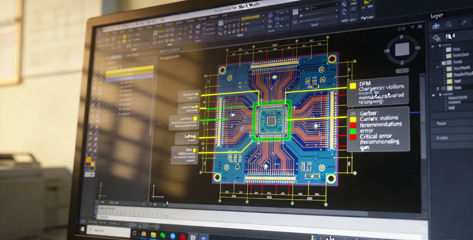
Industrial Electronics operate under conditions that consumer products never face. Temperature extremes, vibration, humidity, and decades of expected service life. When a consumer gadget fails, a warranty return costs money. When an industrial controller fails in a factory, production stops. When a medical device fails, lives are at risk. This is why Industrial Pcb design demands discipline—not optional best practices.
The most expensive PCB is the one you have to remake. Every respin costs more than the previous—it's not linear. A single DFM-caught error before layout saves weeks compared to discovering it after fabrication. Invest the time upfront.
These rules aren't theoretical recommendations. They're the practices that, when followed, consistently produce boards that pass first-pass inspection, survive assembly, and operate reliably in the field.
Every PCB fabricator publishes a capability list—minimum trace width, spacing, via size, layer count, and more. The critical word is "proven." Stating a capability and reliably delivering it are different things. Always design to the comfortable capability range, not the stated maximum. If a fab says they can do 0.1mm traces, design at 0.12–0.15mm unless that specific geometry is essential.
The annular ring is the copper land remaining around a drilled hole. Minimum specification: 0.15mm (6 mil) after drilling. Drill wander—the inevitable positional error in the drilling process—can reduce annular ring by 0.05–0.1mm. Design with margin so that drill wander doesn't create reliability failures or fabrication rejections.
Copper distribution asymmetry is the primary cause of board warpage. When Layer 1 has 80% copper coverage and Layer 4 has 20%, the board will twist during lamination and assembly. Target within 15% copper coverage balance between opposing layers. Add copper thieving patterns to fill low-coverage areas if needed.
Your board doesn't exist in isolation—it will be manufactured as part of a panel. Think about panel utilization from the start. Standard panel sizes (18×24", 21×24") should inform your board dimensions. Include breakaway tabs, mouse bites, or V-grooves in your board outline layer from the beginning, not as an afterthought added after layout is complete.
Clearance is the direct spacing between conductors. Creepage is the path along the surface between conductors. Both matter, but creepage is more sensitive to contamination and humidity. Minimum spacing depends on operating voltage, pollution degree, and applicable safety standards (IEC 60950, IEC 62368, IEC 60601, etc.). Build in margin—50–100% beyond minimum code requirements for industrial designs.
Automated pick-and-place machines need clearance around components. Place SMT components at least 3mm from board edges, 5mm from tall parts, and maintain minimum spacing between adjacent component bodies. Component spacing that is fine for hand assembly becomes a production bottleneck or a source of placement errors for machines.
Every panel needs three global fiducial marks—small cross-hair targets in the panel corners—that give assembly machine vision systems a reference frame. For components with 0.5mm pitch or finer, add local fiducials adjacent to those components. Fiducials cost nothing to add and prevent expensive placement errors. There's no valid reason to omit them.
Designing Test Points after layout is complete typically results in compromised test access—traces that should be probed are buried under components, and Test Points are crowded into unusable locations. Every net that needs electrical verification should have a dedicated test point, minimum 4mm × 4mm. Include test points for power rails, grounds, and critical signal nodes.
The layer stack-up is the most consequential DFM decision in a multi-layer board. It determines impedance, cross-talk, EMC performance, and manufacturing feasibility. Define the stack-up explicitly in your fabrication documentation: number of layers, thickness of each dielectric, copper weight per layer, and target impedance for Controlled Impedance traces. Never leave stack-up to the fabricator's discretion.
Your fabrication documentation is the contract between you and the manufacturer. Vague requirements produce boards that meet someone's interpretation, not yours. Include: material specification (Tg, material grade, UL rating), IPC class level (Class 1, 2, or 3), surface finish type, Solder Mask color and type, Silkscreen requirements, and any special testing or inspection requirements. If it's not documented, don't expect it.
Not every design needs to push the limits of fabrication capability. Understanding your actual requirements—and designing to the appropriate tier—directly controls cost and lead time. Over-specifying capability you don't need is as costly as under-specifying what you do need.
Standard Tier: Trace/Space 0.15mm/0.15mm, Via 0.30mm minimum, BGA Pitch 0.80mm minimum, Thickness Tolerance ±10%, Cost 1× baseline.
Advanced Tier: Trace/Space 0.10mm/0.10mm, Via 0.20mm minimum, BGA Pitch 0.50mm minimum, Thickness Tolerance ±5%, Cost 1.5–2×.
HDI Tier: Trace/Space 0.05mm/0.05mm, Via 0.10mm laser microvia, BGA Pitch 0.30mm minimum, Thickness Tolerance ±3%, Cost 3–6×.
If your design can meet electrical requirements at standard tier geometry, use standard tier. Only push to advanced or HDI capability where the design genuinely requires it. A board that is 95% standard and 5% HDI costs far less than a board that is 100% HDI.
For boards with four or more layers, the stack-up determines everything that follows. A poorly designed stack-up creates EMC problems, Signal Integrity issues, and manufacturing difficulties that no amount of clever routing can fix.
Layer 1 — Component Layer: Primary routing, all surface-mount components.
Layer 2 — Ground Plane: Solid copper, continuous reference for Layer 1 signals. Route nothing here.
Layer 3 — Power and Secondary Routing: Power plane islands with some signal routing capability. Keep power plane as continuous as possible.
Layer 4 — Bottom Routing: Secondary signals and bottom-side SMT components. Route perpendicular to Layer 1 traces to reduce crosstalk coupling.
Before submitting your design files to fabrication, work through this checklist systematically. Each item represents a potential source of delay, rework, or field failure if missed.
After reviewing thousands of PCB designs across dozens of fabrication facilities, certain patterns of DFM failures appear repeatedly. These are the mistakes that are most expensive to fix and most avoidable with proper discipline.
Specifying tolerances two times tighter than your application requires. If your connector fits within ±0.15mm tolerance, specifying ±0.05mm costs money without any functional benefit. Reserve tight tolerances for the specific features that genuinely need them.
Silkscreen designators, polarity marks, and reference indicators aren't decorative—they're assembly documentation. Components placed over silkscreen text create assembly ambiguity. Verify silkscreen legibility by reviewing your design from the assembler's perspective before submission.
Components placed too close to panel edges experience mechanical stress when the board is broken free from the panel. Minimum safe distance: 5mm from any panel edge for breakaway routing. For V-scored panels, components can be closer, but still need to account for the stress of the break.
Modern PCB CAD software includes DFM rule checking. Using it after layout is complete is far better than not using it at all—but using it continuously throughout layout is exponentially more valuable. Configure the rules to match your fabricator's capabilities and run checks at every design milestone, not just before submission.
The relationship between design engineer and PCB fabricator is a partnership. The best outcomes come from fabricators who engage early, communicate clearly, and push back when a design needs adjustment. The cheapest quote is almost never the best value.
What to evaluate: Technical capability match, quality certifications (ISO 9001, AS9100, Iatf 16949), Dfm Review service, traceability documentation, and engineering support responsiveness.
What to avoid: Quotes that are significantly below market rate, fabricators who never push back on designs, and those who can't provide material traceability or quality certifications for industrial applications.
Most reputable fabricators offer Dfm Review—examining your design files before production and flagging potential issues. Use it. The review is typically free or low-cost, and the feedback from an experienced process engineer is worth far more than the price. Submit your design for DFM review before you are 100% complete—early enough to make changes without schedule impact.
Q: When should I engage my PCB fabricator for DFM review?
As early as possible—ideally before layout begins. Share your schematic, proposed stack-up, and any challenging design features. Early engagement identifies potential problems while changes are still cheap to make. Even informal conversations with a fabricator's engineering team before layout starts can prevent significant problems later.
Q: What's the most cost-effective change to improve manufacturability?
Adding fiducial marks. This single addition prevents assembly placement errors that require rework or cause field failures. It costs nothing in board real estate and nothing in fabrication price. Every board should have three global fiducial marks without exception.
Q: How much does DFM optimization affect total product cost?
Studies and industry data consistently show that applying DFM principles early in design reduces total product cost by 20–40% compared to designs that require respins or experience high first-pass failure rates. The ROI is clear: every dollar spent on DFM upfront saves multiple dollars in rework, delays, and warranty costs downstream.
Q: Should I always follow the most conservative DFM rules?
No. Over-engineering has its own costs. Use the rules to understand the trade-offs, then make informed decisions for your specific application. A Class 3 medical device needs maximum conservatism. A low-cost industrial sensor might accept Class 2 tolerances and wider spacing. Match your DFM rigor to your application's actual requirements.
Q: What's the difference between clearance and creepage?
Clearance is the straight-line distance through air between two conductors. Creepage is the shortest path along the surface of the insulating material between conductors. Creepage is almost always larger than clearance for the same voltage rating because surface contamination can create a conductive path along the surface. Safety standards specify both minimum clearance and creepage requirements, and you must satisfy both.
Design It Right. Build It Once.
DFM is not a constraint on creativity—it is the foundation for shipping products that work. Master these rules, develop the habits, and your designs will move from concept to production without the costly detours that plague less disciplined approaches.
Every PCB designer knows the pain. Now you know the solution. Design with manufacturing in mind from the very first schematic, apply these rules systematically, and watch your first-pass yield climb while your development costs fall.
Cost vs. Performance: When to Use HDI Solutions in Industrial DesignSeptember/14/2026

Design for Testability (DFT): A Crucial Aspect of Industrial PCB DesignJuly/20/2026
How to Avoid Costly Mistakes with Proper Industrial PCB DFMJuly/03/2026

The Engineer's Checklist for Industrial PCB DFM Before Sending to FabSeptember/24/2026

Optimizing Trace Width and Spacing in Industrial PCB DFMAugust/06/2026
Design Rules for Heavy Copper Traces in Power ElectronicsJuly/27/2026

Panelization Strategies for Efficient Industrial PCB Design and AssemblySeptember/08/2026
Essential Rules for Industrial PCB DesignJune/08/2026