Open Nav


Industrial printed circuit board assemblies (PCBAs) operate in environments that would destroy consumer electronics within hours. Temperature extremes, continuous vibration, humidity fluctuations, and electromagnetic interference define the operating reality for motor drives, PLC controllers, sensor modules, and power conversion equipment found on factory floors worldwide. The assembly technology choice—surface mount (SMT) or through-hole (THT)—carries consequences that extend far beyond Manufacturing Efficiency into the realm of whether equipment survives or fails in demanding industrial deployments.
This article examines the SMT versus through-hole decision through the lens of industrial application requirements. Rather than abstract technology comparisons, we'll focus on practical best practices that engineers and procurement professionals can apply when specifying or manufacturing Industrial Electronics. The goal is actionable guidance that leads to reliable, cost-effective industrial products.
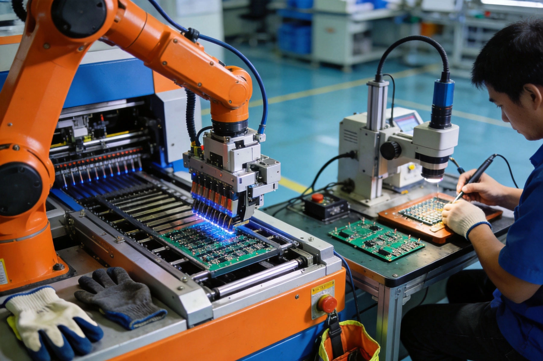

Industrial Electronics occupy a unique position between consumer flexibility and aerospace robustness. They must achieve high reliability at costs compatible with industrial market economics—typically 5-15% annual failure rates that would be unacceptable in medical or aerospace applications, but far below the 20-30% rates common in consumer products. Understanding these requirements helps frame the SMT versus through-hole decision appropriately.
Thermal Cycling exposure represents one of the most significant stressors for industrial equipment. A factory automation controller might experience power-on cycles daily, with each cycle introducing thermal expansion mismatches between component materials. An electric motor drive mounted near heavy machinery endures continuous vibration throughout operation. A outdoor sensor node faces humidity cycling as temperatures change throughout the day. Each failure mechanism interacts with assembly technology choices in specific ways.
Repairability expectations also differ between industrial and consumer markets. Consumer products typically receive no repair—failure means replacement. Industrial equipment, particularly in process industries, often requires field serviceability to minimize downtime. Components that can be replaced by technicians using standard tools, without returning equipment to a service center, shape assembly decisions significantly.
Through-hole technology's fundamental advantage for industrial applications lies in the mechanical bond between component leads and circuit board. Solder joints formed on both board surfaces, with leads passing through drilled holes, create interconnection strength that surface mount technology cannot match without special accommodations.
The mechanical robustness of through-hole solder joints emerges from several factors. The lead insertion through the hole creates a mechanical interlock before soldering—a physical anchor that maintains position during Thermal Cycling. Solder fills the annular ring around the lead, creating a large wetting area that resists pull-out forces. The double-sided soldering provides redundant connection paths that tolerate some degradation before failure occurs.
These characteristics prove particularly valuable for components subject to mechanical stress. Connectors that undergo repeated mating cycles benefit from through-hole mounting that prevents pad lifting. Heavy components like transformers or large capacitors generate significant mechanical loads during vibration that can fatigue surface mount solder joints over time. Power semiconductors dissipating hundreds of watts benefit from the thermal mass and Heat Dissipation paths that through-hole packages typically provide.
Field failure data from industrial equipment supports the mechanical reliability advantage of through-hole for stress-prone applications. Connectors, relays, and electromechanical switches—the components most subject to physical interaction—show significantly lower failure rates when mounted with through-hole technology compared to surface mount equivalents. The failure mode analysis consistently points to solder joint fatigue as the primary surface mount failure mechanism in these applications.
Despite through-hole's mechanical advantages, surface mount technology dominates modern industrial electronics for reasons equally rooted in application requirements. Higher component density enables smaller form factors that industrial equipment increasingly demands. Improved electrical performance from shorter lead lengths benefits high-speed signal paths. Lower manufacturing costs at volume enable competitive pricing that industrial markets require.
The component ecosystem has shifted dramatically toward surface mount packages, particularly for active components. Microprocessors, memory devices, power management ICs, and communication transceivers are simply unavailable in through-hole packages for new designs. Attempting to build a modern industrial controller entirely with through-hole components would either be impossible or require bulky and expensive legacy parts.
Smt Assembly also enables controlled-impedance trace routing that through-hole technology complicates. The ground reference plane discontinuities caused by through-hole barrel plating affect high-speed Signal Integrity in ways that require careful compensation. For industrial Ethernet, fieldbus interfaces, and sensor interfaces operating at elevated frequencies, SMT's cleaner reference plane geometry provides measurable signal quality advantages.
Manufacturing automation benefits further reinforce SMT's dominance. Automated optical inspection (Aoi) detects assembly defects with higher reliability for surface mount components than for through-hole assemblies where solder joints are hidden from top-down inspection views. Automated X-ray Inspection for bottom-side BGAs adds cost but provides defect detection that through-hole Wave Soldering cannot match. These inspection capabilities translate to more consistent field reliability through better defect detection and correction.
Understanding when through-hole technology genuinely improves outcomes enables intelligent selective use rather than reflexive technology commitment.
Electromechanical components subject to physical interaction should almost always use through-hole mounting. Connectors that engineers or operators plug and unplug repeatedly need the Mechanical Strength that through-hole provides. Panel-mount switches, indicator lights, and communication ports that technicians access during maintenance fall squarely in this category.
High-current interconnections above 5-10 amperes benefit from through-hole technology's superior current-carrying capacity and thermal mass. Power input connectors, motor output terminals, and bus bars frequently require through-hole mounting for both electrical and mechanical reasons. The physical size of these components also provides leverage that surface mount pads cannot resist.
Components in high-vibration environments benefit from through-hole mounting when the application places the assembly near rotating machinery or other vibration sources. Without thorough vibration analysis and potentially expensive reinforced mounting schemes, through-hole provides more inherent resistance to vibration-induced failure.
Components with burn-in or screening requirements may be more practically handled in through-hole packages. Military and aerospace screening specifications often reference packages and mounting methods that are more readily adapted to through-hole board designs.
Prototype and low-volume production may benefit from through-hole flexibility. Hand-soldering through-hole components enables faster prototype assembly and easier design changes during development. While modern Smt Assembly handles prototypes efficiently with quick-turn services, through-hole still offers advantages for extreme low-volume or highly iterative development programs.
Surface mount technology should be the default choice for all components not specifically justifying through-hole treatment.
Active components—integrated circuits of any complexity, transistors, and diodes—should use SMT packages almost without exception. The component availability, manufacturing automation, and board density advantages are overwhelming. The occasional through-hole diode or transistor in an otherwise surface-mount design introduces unnecessary assembly process complexity.
Passive components below 0805 package size must use surface mount technology—through-hole alternatives simply do not exist. Even larger passives increasingly use SMT for the same reasons of density and Manufacturing Efficiency that drive active component packaging.
High-speed signal routing benefits from SMT's cleaner geometry. Ethernet PHY chips, high-speed analog-to-digital converters, and precision sensor interfaces all operate more reliably when routed through surface mount packages over continuous reference planes.
Cost-sensitive applications where unit volumes are high and component costs matter should default to surface mount. The manufacturing cost advantage of SMT, particularly at volumes above 1,000 units monthly, directly affects product margins and competitive positioning.
The most practical approach for most industrial PCBAs combines both technologies selectively, applying each where it delivers genuine benefit. This hybrid strategy requires thoughtful implementation to manage the manufacturing complexity it introduces.
Effective hybrid designs typically follow several organizational principles. All surface-mountable components receive SMT treatment. Through-hole components concentrate in specific regions, often near board edges or in mounting zones, where Wave Soldering access is straightforward. The board stack-up accommodates both technologies—typically with sufficient thickness (0.8mm minimum) to ensure wave solder process capability for through-hole sections.
Panelization strategies must account for both assembly processes. Wave solder compatible panel designs include Via-in-pad protection and component orientation rules that prevent solder bridging. SMT panel designs optimize for reflow oven throughput. Combined panels must balance these requirements, sometimes accepting compromises in one process to enable the other.
Component placement planning considers process interactions. Through-hole components must be placed before SMT assembly if both processes share the same reflow cycle. Alternatively, through-hole components can be hand-assembled or selectively soldered after SMT completion. The assembly sequence must be documented and followed consistently to ensure reliable solder joints from both processes.
Regardless of assembly technology, industrial applications demand Solder Joint Reliability exceeding consumer product expectations. Several best practices address this requirement.
Lead-free solder considerations have become unavoidable for most industrial equipment, as environmental regulations increasingly mandate RoHS compliance. Lead-free alloys, typically tin-silver-copper (SAC) formulations, exhibit different mechanical properties than traditional tin-lead solders. They are more susceptible to void formation, tin whisker growth, and mechanical shock sensitivity. Industrial applications using lead-free assembly should verify Solder Joint Reliability through accelerated thermal cycling testing, not just accepting standard assembly processes.
Thermal cycling qualification validates that specific board assemblies survive expected field conditions. IPC specifications provide baseline guidance, but industrial equipment often requires extended testing beyond standard requirements. Define your thermal cycling requirements based on actual field conditions, then qualify assemblies to those requirements through testing rather than assuming standard processes will suffice.
Conformal Coating application significantly improves solder joint reliability in humid or corrosive environments. The coating seals joints against moisture and contamination that accelerate failure mechanisms. Industrial equipment destined for outdoor or process-industry environments should specify Conformal Coating as standard practice, regardless of assembly technology.
Vibration testing becomes necessary when assemblies operate in high-vibration environments. Through-hole components may still fail in extreme vibration despite their inherent mechanical advantage. Testing to actual vibration levels reveals whether design accommodations—mounting holes, reinforcement brackets, or potting—become necessary.
Industrial Pcba design must balance manufacturing efficiency against field reliability in ways that sometimes conflict with pure cost optimization.
Pad size and spacing for both SMT and through-hole should accommodate manufacturing tolerances while maintaining adequate design margin. Industrial products typically have longer manufacturing lifecycles than consumer products, and manufacturing process improvements or supplier changes can shift tolerances over time. Designing adequate margin at the outset prevents field problems from manufacturing drift.
Test point accessibility deserves explicit attention during layout. Industrial equipment often requires in-circuit testing, Boundary Scan testing, and functional verification during manufacturing and field service. Test Points must be accessible with standard probe sizes and spaced to avoid interference from tall components. Adequate test access reduces manufacturing cost and enables field service diagnostics that minimize downtime.
Documentation for serviceability should accompany every Industrial Pcba design. Components subject to field replacement require clear identification, access provisions, and appropriate mounting methods. Silkscreen markings should include reference designators, component values, and polarity indicators that service technicians can read in poorly lit enclosures. Assembly drawings should specify repair procedures and torque values for critical fasteners.
Bom Management practices differ between industrial and consumer products. Industrial products often remain in production for 10-15 years, requiring BoM stability that consumer markets don't demand. Component second-source qualifications should occur during initial design, not as emergency responses to obsolescence notices. Designing-in preferred components with multiple qualified sources prevents production interruptions that industrial customers find unacceptable.
Industrial PCBA manufacturing involves process choices that affect both cost and reliability.
Wave soldering versus Selective Soldering for through-hole components presents a decision that depends on board complexity and production volume. Wave soldering processes entire boards through a molten solder wave, providing fast throughput for simple through-hole boards. Selective Soldering targets specific joints with localized solder application, enabling mixed-technology boards where some through-hole components would be damaged by full wave exposure. The choice balances throughput against process flexibility.
Reflow profile optimization for SMT components affects both manufacturing yield and field reliability. Lead-free assemblies require higher peak temperatures and longer time-above-liquidus than traditional tin-lead processes. These requirements stress the board, components, and solder joints in ways that optimized profiles can minimize. Profile development should include thermocouple mapping across the board to identify temperature variations that could cause defects.
Aoi and X-ray Inspection capabilities vary between manufacturers and should factor into supplier selection. Standard AOI effectively detects most surface mount defects. BGAs, QFNs, and other bottom-terminated components require X-ray inspection for reliable defect detection. Industrial assemblies benefit from full inspection coverage, particularly for components where solder joint quality directly affects field reliability.
Industrial PCBA costs accumulate across design, manufacturing, and field service phases. Optimizing only manufacturing cost often increases total cost when field failure rates or serviceability suffer.
Component selection drives the majority of PCBA cost in most designs. Intelligent component selection—choosing parts with good availability, multiple sources, and proven manufacturing history—prevents production delays and price spikes that affect final assembly cost. Avoid single-source components whenever possible, even at some cost premium.
Design For Testability reduces manufacturing cost by enabling efficient defect detection and diagnostic processes. Boards with good Dft features—Boundary Scan access, Test Points for critical nodes, powered-test capability—yield lower cost-per-good-unit at final test. The design cost to implement Dft features pays back through manufacturing efficiency.
Panelization efficiency directly affects manufacturing cost for surface mount assemblies. Designs that optimize board size relative to standard panel dimensions reduce waste and improve throughput. Work with your contract manufacturer to determine optimal panel utilization before finalizing board dimensions.
Volume commitments significantly affect unit pricing for industrial assemblies. Raw material costs dominate component expenses, and component suppliers offer pricing breaks for volume commitments. Manufacturing setup costs amortize more favorably across larger production runs. However, avoid over-committing to volumes that exceed actual demand—industrial inventory carrying costs and obsolescence risk can outweigh unit price savings.
Industrial PCBA quality depends heavily on Manufacturing Partner Selection and ongoing relationship management.
Process capability verification should precede production commitments. Request capability studies demonstrating that the supplier can achieve your tolerances, not just your specifications. Specifications describe acceptable outcomes; capability studies verify that processes consistently achieve those outcomes. Cpk measurements for critical parameters should exceed 1.33 minimum, with targets above 1.67 for more demanding requirements.
Quality system certification provides baseline assurance of process control. ISO 9001 certification indicates general quality management maturity. Industry-specific certifications—Iatf 16949 for automotive, AS9100 for aerospace, ISO 13485 for medical—demonstrate deeper capability in regulated environments. For industrial equipment, ISO 9001 with demonstrated IPC-A-610 workmanship compliance often suffices, but assess your specific requirements.
First Article Inspection (FAI) validates that initial production runs meet all specifications. Require FAI reporting for new product introduction, following AS9102 requirements or equivalent. This inspection confirms that manufacturing processes achieve design intent before production scales to volume levels.
Ongoing quality monitoring tracks performance over production lifetime. Defect rates, first-pass yield, field failure reports, and customer complaints all provide quality data that should flow back to manufacturing improvement initiatives. Choose suppliers who view quality as Continuous Improvement opportunity rather than acceptable defect rate compliance.
Experience from industrial PCBA programs reveals recurring mistakes that quality-focused teams should avoid.
Over-specifying technology requirements drives unnecessary cost when simpler approaches would suffice. Not every industrial application requires exotic materials, ultra-fine pitch components, or advanced HDI processes. Evaluate actual requirements honestly, then specify minimum necessary technology rather than maximum capability.
Underestimating Thermal Management leads to premature field failures. Power dissipation calculations should drive heat sink specifications, Thermal Via placement, and airflow design. Assuming that packages will operate within ratings without explicit thermal analysis invites failures in production units that happen to run at high ambient temperature or low airflow conditions.
Neglecting EMI hardening causes field problems in industrial environments with high electromagnetic interference. Grounding practices, shield coverage, and trace routing for sensitive signals should receive explicit design attention. Industrial EMC requirements often exceed consumer specifications—designing to consumer levels invites field failures when industrial interference sources appear.
Failing to plan for obsolescence creates production crises years after initial design. Component lifecycle planning should identify likely obsolescence candidates and plan second-source qualifications or lifetime buys before production demands force hasty decisions. Industrial products that remain in production for 10-15 years will inevitably face component discontinuation—planning for this reality avoids crisis management.
Industrial equipment field serviceability should influence design decisions significantly, particularly for equipment where downtime carries high costs.
Component accessibility affects service repair times and technician frustration. Components likely to require field replacement should mount on accessible surfaces with adequate clearance for removal tools. Avoid mounting components under other components or behind hardware that requires extensive disassembly.
Repair procedure documentation should accompany every product, specifying solder iron temperatures, preheat requirements, and inspection criteria for field repairs. These procedures ensure that repairs meet quality standards regardless of technician skill level. Poorly executed field repairs often cause worse problems than the original failure.
Spare parts management requires balancing inventory costs against repair response capability. Popular components prone to failure should stock at field service locations. Rarely-failed components may stock centrally or ship from suppliers on demand. The service parts strategy should align with overall product service level commitments.
Industrial PCBA technology continues evolving, with several trends shaping future practice.
Miniaturization pressure pushes industrial equipment toward smaller form factors, requiring finer-pitch components and more sophisticated HDI techniques. Even traditionally conservative industrial designs increasingly adopt packaging technologies previously limited to consumer electronics.
Integration trends consolidate functions that previously required separate components onto single IC packages or system-in-package solutions. This integration reduces component count and board complexity while increasing the consequences of any individual component failure.
Embedded component technology may eventually enable passive components embedded within the PCB structure itself, eliminating surface mount passives and reducing board area further. While still emerging, embedded technologies could reshape industrial PCBA practice over the coming decade.
Supply Chain Resilience has gained prominence following recent disruption events. Geographic diversification of component sources, increased inventory buffers, and second-source qualification urgency all reflect lessons learned from recent shortages. Industrial PCBA strategies increasingly incorporate supply chain risk management alongside traditional cost and quality optimization.
The SMT versus through-hole decision for industrial PCBA ultimately reduces to matching technology characteristics to application requirements. Neither technology is universally superior—each excels in specific contexts. The best industrial designs apply technology selection criteria derived from field conditions, manufacturing capabilities, and lifecycle expectations. Through-hole where mechanical robustness genuinely matters, surface mount everywhere else, combined with thoughtful hybrid implementation when both technologies appear justified. This pragmatic approach, backed by thorough qualification and supplier partnership, produces industrial assemblies that survive demanding deployment conditions at costs compatible with industrial market economics.
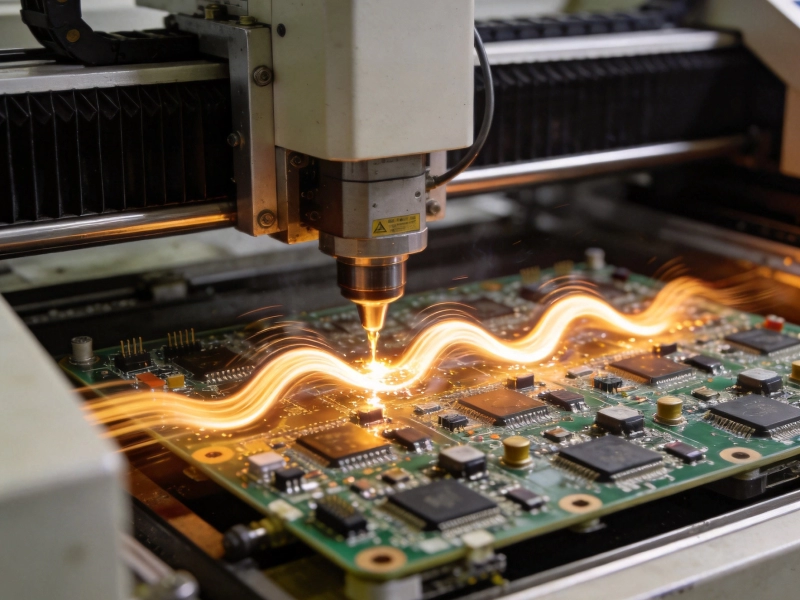
Selective Soldering Techniques for Mixed-Technology Industrial PCBA<September/09/2026
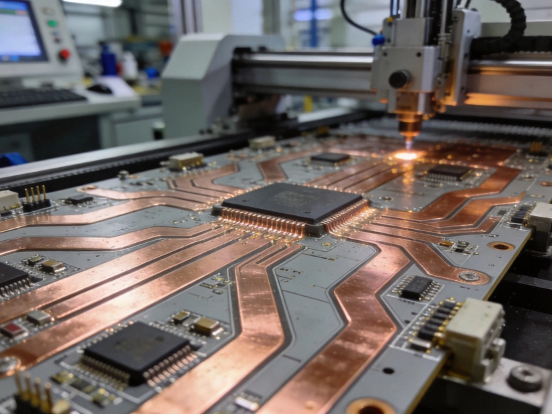
Manufacturing Processes for Extreme Heavy Copper Industrial PCBsAugust/15/2026
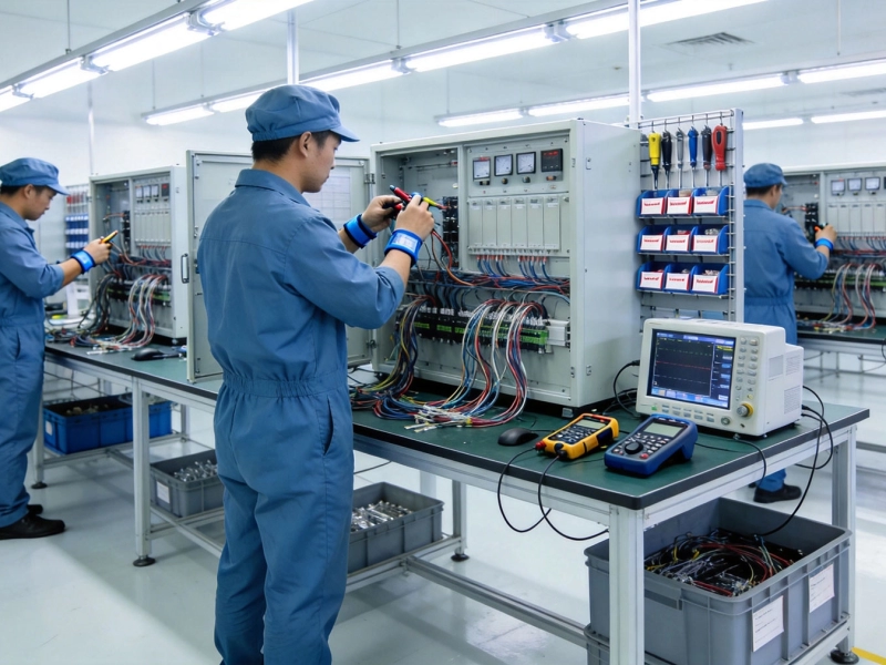
Navigating the Complexities of Box Build AssemblyMay/27/2026
How to Ensure Quality Control in High-Mix Low-Volume Industrial PCBAJuly/21/2026
X-Ray Inspection: Why It's Vital for Complex Industrial PCBA ProjectsSeptember/26/2026
The Importance of Component Obsolescence Management in Industrial PCBAAugust/07/2026
Industrial PCBA: Navigating the Complexities of Box Build AssemblyJune/09/2026
Heavy Copper PCBs: The Solution for High-Current Industrial ApplicationsJune/18/2026