Open Nav


The industrial pcb manufacturing landscape is undergoing a profound transformation in 2026. Powered by advances in artificial intelligence, machine learning, robotics, and smart factory technologies, automation is reshaping every aspect of PCB production, from initial design verification to final assembly and testing. What was once a labor-intensive industry with significant variability is rapidly becoming a high-precision, data-driven operation where machines, software, and human expertise work together to achieve results that were unthinkable just a decade ago.
For electronics manufacturers, the implications are significant: higher yields, lower defect rates, faster production cycles, reduced labor costs, and the ability to produce increasingly complex PCBs at scale. But the automation revolution in PCB production is about more than just cost and speed—it is fundamentally changing what is possible in Electronics Design, enabling miniaturization, advanced packaging, and feature densities that push the boundaries of what traditional manufacturing processes can achieve.
This article explores the key automation technologies driving this transformation, their impact on PCB production, and what manufacturers need to know to stay competitive in this rapidly evolving landscape.
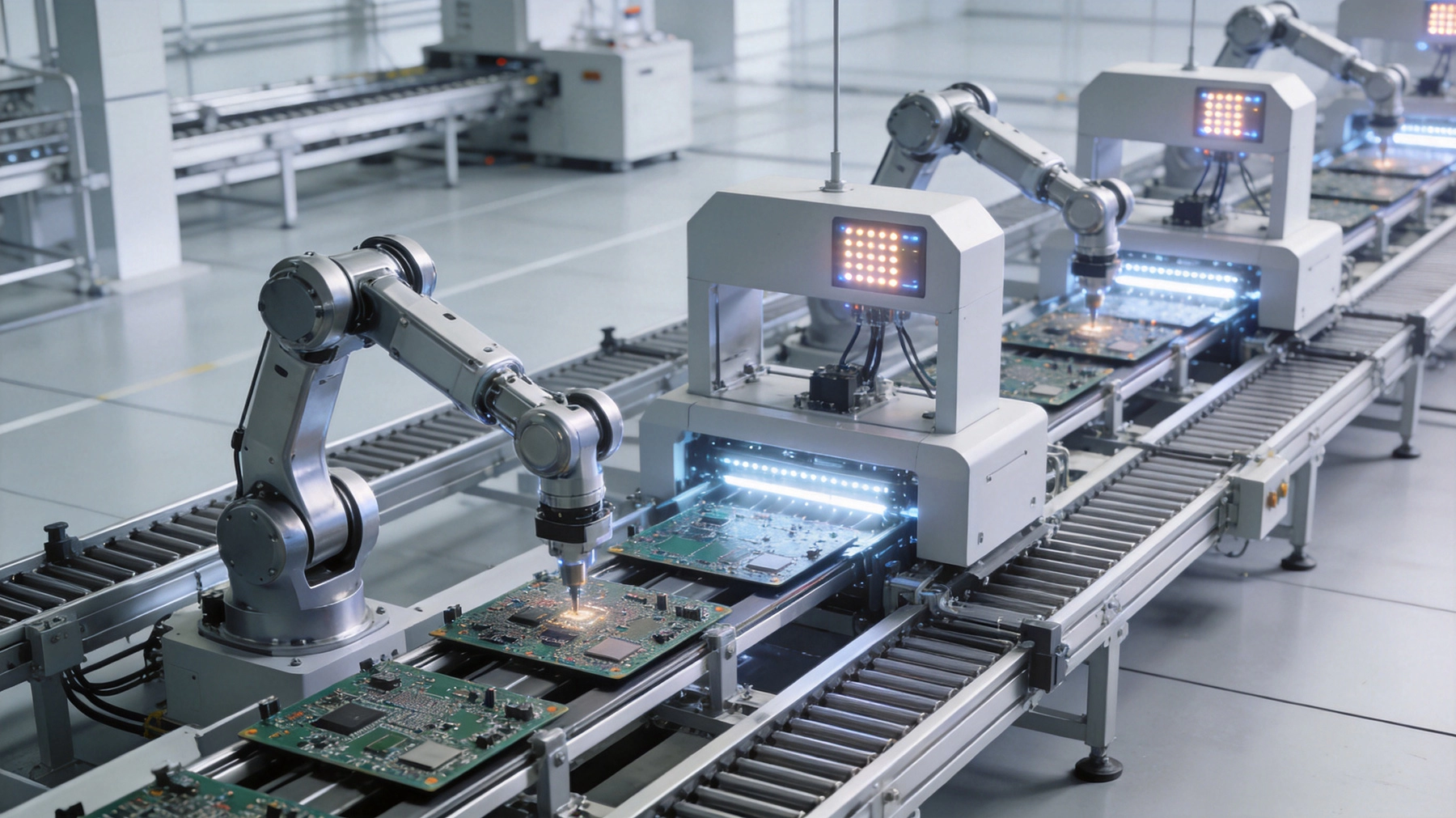
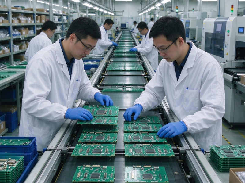
To appreciate the scale of the transformation underway, it helps to understand the limitations of traditional PCB production. Conventional Pcb Manufacturing has long been a hybrid process, combining automated equipment like CNC drilling machines and reflow ovens with significant manual intervention at many stages. Human operators performed visual inspections, handled component placement on complex or irregular boards, managed material handling, and conducted quality checks that required judgment and experience.
This hybrid approach had several inherent limitations. First, there was significant variability in output quality, even with experienced operators. Subtle differences in technique, attention, and fatigue could affect defect rates from shift to shift or operator to operator. Second, the process was slow and resource-intensive, with many stages requiring significant time for setup, execution, and inspection. Third, as PCB designs became more complex—higher layer counts, finer trace widths, smaller components, advanced packaging like BGAs and QFNs—the limitations of manual processes became increasingly apparent.
In 2015, typical defect rates in PCB production ranged from 500 to 2,000 DPPM (defects per million units), with even the best manufacturers struggling to consistently achieve rates below 200 DPPM. Production cycles for complex multi-layer boards could take 10-15 days or more. By 2026, leading automated facilities have achieved defect rates below 50 DPPM and production cycles as short as 3-5 days for comparable boards—a transformation that is largely driven by automation.
One of the most impactful applications of AI in PCB production is automated optical inspection (Aoi) and X-ray Inspection enhanced with deep learning algorithms. Traditional Aoi systems used rule-based algorithms to detect defects by comparing captured images against reference images. While effective for obvious defects, these systems had high false positive rates and struggled to detect subtle or complex defects that did not fit predefined rules.
AI-powered AOI systems in 2026 use convolutional neural networks (CNNs) and transformer-based vision models trained on millions of PCB images to detect defects with human-level or superhuman accuracy. These systems can identify issues such as solder bridges, insufficient solder, tombstoning, component misalignment, scratches, and contamination with far greater accuracy than traditional systems, while also dramatically reducing false positive rates that lead to unnecessary rework and inspection time.
More importantly, AI inspection systems improve continuously over time. As they process more boards, they learn from new data, becoming more accurate at detecting both common and rare defects. This continuous learning capability means that defect detection accuracy actually improves as the system is used, rather than degrading or stagnating as with traditional systems.
X-ray Inspection for hidden defects in BGA and QFN packages has similarly been transformed by AI. Automated X-ray systems with AI can now detect voiding in solder joints, cracked die, and Delamination with accuracy that rivals destructive cross-section analysis, but at production speeds and without destroying the board.
Automation in 2026 has moved well beyond simple machine control to intelligent, self-optimizing processes. Modern PCB production equipment is equipped with an array of sensors that continuously monitor key process parameters—temperature profiles in reflow ovens, drill speeds and feeds, plating bath chemistry, solder paste viscosity, and hundreds of other variables.
Machine learning algorithms analyze this sensor data in real time, identifying patterns that indicate process drift or impending equipment failures before they cause defects. For example, a slight increase in drill torque might indicate a dull drill bit that is about to cause drill breakage or board damage. An AI system can detect this pattern and alert maintenance teams to replace the drill before a failure occurs, preventing costly downtime and defective boards.
Predictive maintenance has been particularly impactful for high-cost equipment like Laser Drilling machines, electroplating lines, and automated optical shapers. By predicting equipment failures days or weeks in advance, manufacturers can schedule maintenance during planned downtime rather than experiencing unexpected breakdowns that halt production and create backlogs. In 2026, leading manufacturers report up to 60% reduction in unplanned equipment downtime through predictive maintenance.
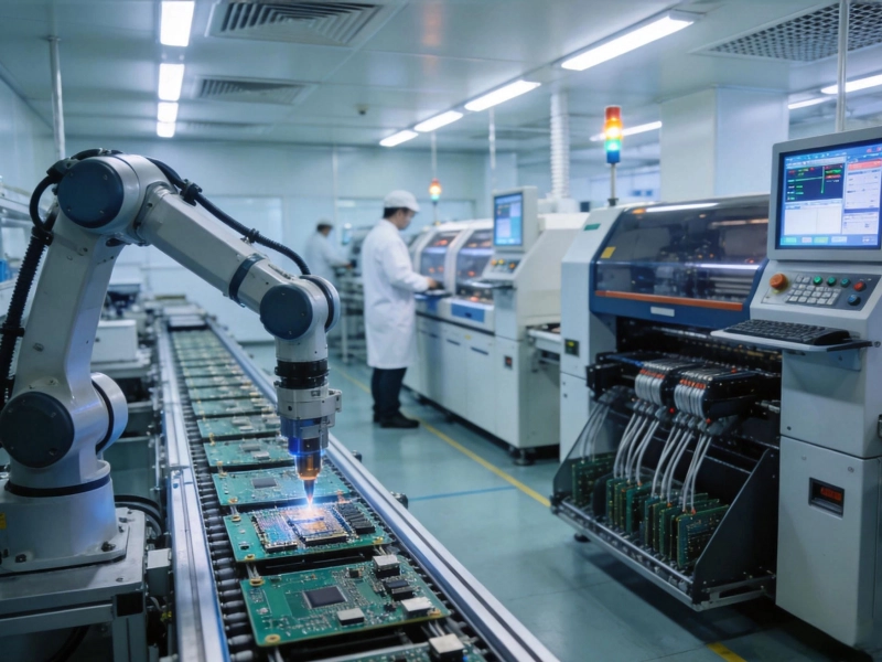
Robotics has transformed material handling in PCB production, which was historically one of the most labor-intensive and error-prone stages. Modern automated PCB facilities in 2026 use a combination of industrial robots, automated guided vehicles (AGVs), and conveyor systems to move materials, work-in-progress boards, and finished products throughout the facility with minimal human intervention.
Automated storage and retrieval systems (AS/RS) manage raw materials like laminate sheets, prepregs, and Copper Foil with precise inventory tracking. Robotic arms handle panel loading and unloading at key production steps, and automated inspection stations. AGVs transport materials between production areas, guided by real-time location systems that optimize routing and minimize congestion.
The impact on quality is significant. Automated material handling reduces the risk of board damage from manual handling—scratches, bent boards, and contamination from fingerprints are virtually eliminated. It also improves consistency and reduces contamination risks, as automated systems do not introduce the variability and contaminants that human handling can introduce.
Component placement accuracy has improved dramatically with the latest generation of automated pick-and-place machines. Modern placement systems in 2026 achieve placement accuracies of ±0.01mm or better, enabling reliable placement of 01005 components (0.4mm × 0.2mm), fan-out wafer-level packages (FOWLP), and other advanced packages that are increasingly common in modern electronics.
These systems use machine vision and AI to verify component orientation, solder paste coverage, and placement accuracy in real time, making adjustments on the fly to compensate for variations in component dimensions, board warpage, or other factors. The integration of AI allows these systems to optimize placement sequences for speed and accuracy, learning from each board to improve performance over time.
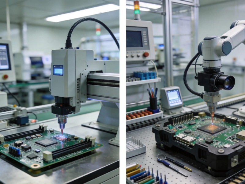
For the most advanced packaging technologies like embedded components, 2.5D and 3D stacking, and chip-on-board assemblies, specialized automation systems have been developed that handle the unique challenges of these technologies. These systems can place and bond bare die, handle ultra-thin wafers, and perform precision dispensing of adhesives and encapsulants—all with levels of precision and consistency that manual processes cannot match.
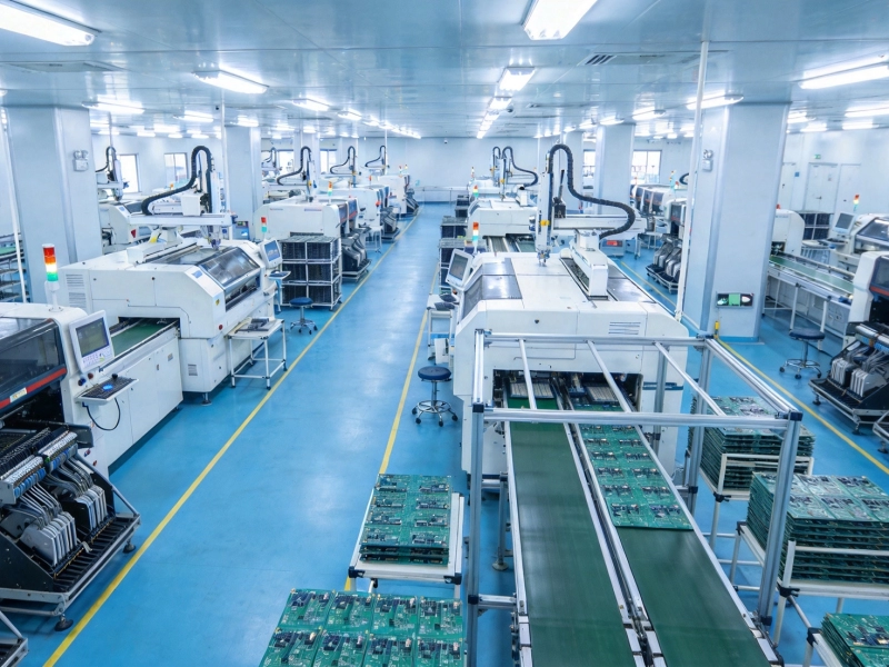
The concept of the smart factory—where every aspect of production is connected, monitored, and optimized through digital systems—has become a reality in leading Pcb Manufacturing facilities in 2026. Every machine, process, and quality check is connected through an industrial IoT (IIoT) network that feeds data into a central manufacturing execution system (MES) and enterprise resource planning (ERP) system.
Digital twin technology has emerged as a powerful tool for Pcb Production Optimization. A digital twin is a virtual replica of the production process that is continuously updated with real-time data from sensors and production systems. Engineers can use the digital twin to simulate process changes, test new production recipes, and optimize parameters without disrupting actual production.
For example, before changing the reflow temperature profile for a new board design, engineers can simulate the impact on the digital twin to verify that the new profile will produce good solder joints without causing component damage. This reduces the risk of production errors and allows optimization that would be impractical or too risky to experiment with on actual production equipment.
Automation has also transformed the design stage of PCB production. Advanced DFM software in 2026 uses AI to analyze design files and identify potential manufacturability issues before production begins. These systems can detect hundreds of potential issues—from trace width violations and insufficient clearances to problematic via structures and component placement conflicts—with recommendations for resolution.
Some advanced DFM systems go beyond simple rule checking to use generative AI to suggest design modifications that improve manufacturability while maintaining the original design intent. For example, if a design has trace widths that are too narrow for the manufacturer's capabilities, the system can suggest alternative routing strategies that achieve the same electrical performance with wider traces that are easier to manufacture.
The automation revolution in PCB production has produced measurable improvements across every key production metric:
Perhaps the most significant impact of automation has been on defect rates and yield. As of 2026, leading automated PCB facilities consistently achieve defect rates below 50 DPPM, compared to 200-500 DPPM at facilities relying on traditional processes. For some high-volume, relatively simple board types, defect rates below 10 DPPM are achievable. This dramatic improvement in quality translates directly to lower costs, as less material is wasted on defective boards, and fewer customer returns and warranty claims are incurred.
Automation has significantly increased production throughput. Automated lines can operate continuously 24/7 with minimal human intervention, removing the breaks, shift changes, and fatigue limitations that constrain human operators. Advanced scheduling algorithms optimize production sequencing to maximize equipment utilization and minimize changeover times. Overall, automated facilities in 2026 typically achieve 40-60% higher throughput than equivalent manual facilities for the same board types.
Lead times for complex multi-layer boards have been compressed from 10-15 days to 3-5 days at fully automated facilities, and quick-turn prototype services can now deliver boards in 24-48 hours for standard designs. This dramatic reduction in lead times is enabled by optimized process flows, reduced inspection and rework times, and faster equipment changeovers—all driven by automation.
While automation has reduced the number of direct labor positions in PCB manufacturing, it has simultaneously created new, higher-skilled roles for automation engineers, data scientists, and robotics technicians. The net effect has been a shift toward higher-value work and improved labor productivity. Facilities that once required 50 operators to produce 10,000 boards per month now achieve the same output with 15-20 operators supported by automation systems, while producing higher quality boards with shorter lead times.
Automated production systems generate comprehensive records of every process step, inspection result, and material lot used in each board. This complete traceability is invaluable for quality management, regulatory compliance, and customer support. When a quality issue arises, manufacturers can trace the exact conditions under which a board was produced, identify the root cause quickly, and take corrective action before the issue affects additional boards.
Despite the clear benefits of automation, adopting these technologies presents real challenges for PCB manufacturers:
Automated PCB production lines require significant capital investment. A modern automated AOI system can cost $200,000-$500,000, an advanced pick-and-place line can cost $1-3 million, and a fully integrated smart factory implementation can require tens of millions of dollars in investment. For smaller manufacturers, this barrier to entry is significant, and many are turning to automation-as-a-service models or shared manufacturing facilities to access these capabilities without bearing the full capital cost.
Automation requires a fundamentally different skill set than traditional PCB manufacturing. Workers need to be comfortable with digital systems, robotics, and data analysis, rather than manual assembly techniques. Transitioning an existing workforce to these new skills takes time and investment, and some workers may not be able to make the transition. Manufacturers must invest in training and development while also recruiting new talent with the necessary digital skills.
Bringing together diverse automation systems—equipment from different vendors, IIoT sensors, MES systems, AI inspection software—into a coherent, integrated smart factory is a significant technical challenge. Data formats, communication protocols, and system architectures often differ between vendors, requiring extensive integration work. Manufacturers need strong IT and engineering teams to manage this complexity.
AI and machine learning systems are only as good as the data they are trained on. Many manufacturers have accumulated years of production data, but in inconsistent formats, with missing values, or in systems that are difficult to access. Building the data infrastructure to support AI-powered automation requires significant effort in data collection, cleaning, and organization.
Despite the remarkable advances in automation, human expertise remains essential to PCB production in 2026. Automation excels at repetitive, data-driven tasks, but human judgment is still critical for handling unusual situations, solving complex problems, and making strategic decisions.
Process engineers apply their experience and intuition to interpret AI recommendations, decide when to trust automated decisions and when to apply human judgment, and continuously improve processes based on their understanding of the underlying physics and chemistry of PCB manufacturing. Quality engineers investigate complex defect patterns that AI systems flag and determine appropriate corrective actions. Design engineers collaborate with manufacturers to optimize designs for manufacturability and leverage new automation capabilities.
The most successful manufacturers in 2026 have found the right balance between automation and human expertise, using automation to handle routine, high-volume tasks while deploying human talent where judgment, creativity, and problem-solving are most valuable. This human-machine collaboration model produces results that neither humans nor machines could achieve alone.
The automation of PCB production is still in its early stages, and the next wave of advances is already on the horizon:
Automation is fundamentally transforming Industrial Pcb production in 2026, delivering dramatic improvements in quality, speed, cost, and capability that are reshaping the industry. Manufacturers who embrace these technologies are achieving defect rates, production speeds, and flexibility that were unimaginable just a decade ago, while those who lag behind face an increasingly difficult competitive position.
The automation revolution is not just about replacing manual labor with machines—it is about creating a new paradigm for manufacturing that combines the consistency and speed of machines with the judgment and creativity of human expertise. Manufacturers that master this human-machine collaboration will be best positioned to thrive in the rapidly evolving Electronics Manufacturing landscape of the coming decade.
For electronics product companies, the implications are clear: the PCB manufacturers you partner with should be investing aggressively in automation, and your supply chain strategy should account for the growing gap between highly automated and traditional manufacturers. In a world where automation is reshaping every aspect of Electronics Production, partnering with the right manufacturer is more important than ever.
A: No, while automation handles many routine tasks, human expertise remains essential for process optimization, problem-solving, design collaboration, and managing complex situations. The most successful facilities use automation and human workers in complementary roles, with automation handling repetitive, high-volume tasks and humans focusing on judgment-intensive activities.
A: Full automation of an existing production line is typically a multi-year process that involves incremental investments, workforce training, and process redesign. A phased approach—automating one process at a time, validating results, and expanding—is usually more practical than attempting a complete transformation at once. Most manufacturers should plan for a 3-5 year roadmap for comprehensive automation.
A: The ROI for automation varies by application, but many automated systems pay for themselves within 1-3 years through reduced labor costs, lower defect rates, higher throughput, and reduced scrap. For high-volume production lines, the payback can be even faster. However, accurate ROI calculations must account for the full cost of ownership, including maintenance, training, and integration.
A: Smaller manufacturers face real challenges in accessing automation, but new models like automation-as-a-service, shared manufacturing facilities, and cloud-based AI inspection services are making advanced automation more accessible. Rather than investing millions in their own equipment, smaller manufacturers can access these capabilities on a pay-per-use basis, leveling the playing field.
Understanding the Lifecycle of an Industrial PCB Production RunJuly/31/2026
How to Scale Your Industrial PCB Production for Mass ManufacturingJune/02/2026
5 Critical Steps to Optimize Your Industrial PCB Production WorkflowJuly/15/2026
Navigating Supply Chain Challenges in Global Industrial PCB ProductionOctober/14/2026
Key Differences Between Consumer and Industrial PCB ProductionJune/27/2026
The Complete Guide to Manufacturing Processes and Industry ChallengesMay/27/2026
Cost Reduction Strategies in High-Volume Industrial PCB ProductionSeptember/18/2026
Via-in-Pad and Microvias: Key Features of Advanced HDI SolutionsJuly/26/2026