Open Nav


When signals travel through a printed circuit board at high frequencies, the behavior of those signals depends critically on the impedance of the traces carrying them. Impedance mismatches cause reflections that corrupt signal integrity, create electromagnetic interference, and can render a high-speed design non-functional. Controlling impedance is not optional in modern Industrial Electronics. It is a fundamental requirement for reliable operation.
This article covers the practical aspects of impedance control in high-frequency PCB designs targeted at industrial applications. From understanding what impedance means in a transmission line context to implementing controlled impedance in your stack-up, these principles apply whether you are designing a motor drive controller, a communication module, or a precision sensor interface.
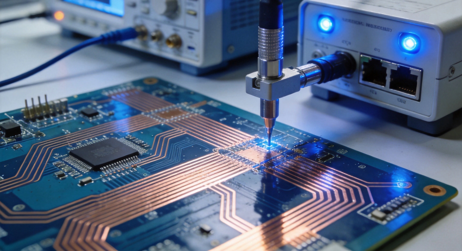
Characteristic impedance is the ratio of voltage to current for a signal propagating along a transmission line. It is determined by the physical geometry of the trace and its relationship to reference planes, not by the length of the trace or the termination components at the ends. For a simple microstrip trace, a conductor over a ground plane, the characteristic impedance depends on trace width, copper thickness, dielectric thickness, and the Dielectric Constant of the substrate material.
The key insight is that when a signal encounters a change in impedance, part of the signal reflects back toward the source. The magnitude of reflection depends on the impedance mismatch. A fifty ohm trace that suddenly transitions to seventy-five ohms will reflect a portion of the signal energy. In digital systems, these reflections show up as ringing, overshoot, and undershoot on signal edges. In analog RF systems, reflections reduce power transfer and distort frequency response.
Controlled impedance PCBs most commonly target fifty ohms for single-ended signals and one hundred ohms for differential pairs. The fifty ohm standard emerged from coaxial cable development in the early twentieth century as a compromise between power handling and attenuation. For PCB traces, fifty ohms is also relatively easy to achieve with reasonable trace widths on standard board materials.
One hundred ohms for differential pairs similarly balances practical geometry against signal integrity requirements. Differential signaling, where information is encoded in the voltage difference between two traces rather than between a single trace and ground, offers common mode noise rejection and reduced electromagnetic emissions. The differential impedance depends on both the single-ended impedance of each trace and the coupling between them.
Microstrip is the simplest transmission line structure. A signal trace runs on the outer layer of the board, separated from a ground plane on the layer below by the dielectric substrate. Microstrip is easy to fabricate and easy to probe for testing, but it has disadvantages for high-frequency applications. The exposed trace radiates more electromagnetic energy than embedded structures, and the effective Dielectric Constant is a mixture of the board material and air above the trace, making impedance more sensitive to manufacturing variations in Solder Mask thickness.
Microstrip impedance calculations must account for the Solder Mask coating. Mask adds a thin dielectric layer on top of the trace that lowers the effective impedance slightly. Without including mask in the calculation, fabricated boards may measure five to ten percent lower impedance than designed.
Stripline places the signal trace between two ground planes, embedded within the board substrate. This structure provides better electromagnetic shielding than microstrip and more consistent impedance because the trace is completely surrounded by the board dielectric. Stripline is preferred for the highest frequency applications and for signals that must not couple to adjacent traces.
The tradeoff is that stripline requires more layer count to implement. A four-layer board can only support microstrip on the outer layers. Stripline requires at least six layers to have two ground planes with signal layers between them. Stripline traces are also harder to access for probing and troubleshooting.
Coplanar waveguide places ground planes on the same layer as the signal trace, alongside it rather than below it. This structure can achieve controlled impedance with thinner dielectrics than microstrip, and the ground-signal-ground configuration provides good isolation between adjacent signals. Coplanar waveguide is common in RF applications and in situations where board thickness cannot accommodate the dielectric height required for microstrip.
Simple formulas exist for calculating microstrip and stripline impedance given geometry and material properties. The IPC-2141 standard provides widely used approximations. However, these formulas make simplifying assumptions about field distributions and become less accurate for extreme geometries like very wide traces over thin dielectrics.
Field solver software solves Maxwell equations numerically to calculate impedance more accurately. Modern Pcb Design tools integrate two-dimensional field solvers that account for trace shape, solder mask, adjacent traces, and other real-world factors. For critical designs, investing time in field solver analysis pays dividends in first-pass success.
No manufacturing process produces exactly the designed geometry. Trace width varies due to etching undercut. Dielectric thickness varies between different laminate lots. Dielectric constant varies with resin content and glass weave. The result is that fabricated impedance has a statistical distribution around the design target.
Standard PCB fabrication processes target impedance within plus or minus ten percent of the design value. Tighter tolerances of five percent or better require additional process controls and increase cost. When specifying impedance, include both the target value and the acceptable tolerance. A specification of fifty ohms plus or minus ten percent gives the manufacturer clear guidance on what is acceptable.
Every controlled impedance trace needs a continuous reference plane. For single-ended signals, this is typically a ground plane on an adjacent layer. For differential pairs, the reference can be ground or power, though ground is preferred for signal integrity. The reference plane provides the return path for signal current, and any discontinuity in the reference plane creates an impedance discontinuity in the trace.
Reference plane voids, where copper is removed from the plane, must be avoided under high-speed traces. If a trace must cross a split in a reference plane, provide a stitching capacitor or modify the routing to maintain continuous reference. Crossing plane splits is a common source of signal integrity problems that shows up as excessive emissions or unexpected ringing.
Controlled impedance layers should be positioned adjacent to reference planes. In a standard six-layer board, layers one and six are microstrip with reference on layers two and five respectively. Layers three and four form a stripline pair with references on layers two and five. This configuration provides controlled impedance on all signal layers.
For high layer count boards, symmetric stack-ups are preferred. Place signal layers in pairs with a reference plane between them. This creates two stripline layers per reference plane trio and maintains mechanical balance to prevent board warpage. Avoid asymmetric stack-ups where all controlled impedance layers are on one side of the board centerline.
The dielectric constant of the substrate directly impacts impedance. Higher dielectric constant means lower impedance for the same geometry, or narrower traces for the same impedance. Standard FR-4 has dielectric constant around 4.5 at low frequencies, dropping to approximately 4.2 at gigahertz frequencies due to dispersion.
For high-frequency applications, low-loss materials like Rogers RO4000 series or Isola I-Tera offer more stable dielectric constants and lower loss tangents than standard FR-4. These materials cost more but provide better signal integrity at microwave frequencies. When using specialized materials, verify that the PCB fabricator has experience processing them, as they may require different drilling, plating, and etching parameters than standard FR-4.
Width is the primary adjustment variable for impedance control. Given fixed dielectric thickness and material, narrower traces have higher impedance. The relationship is approximately logarithmic. Doubling trace width might only change impedance by twenty percent rather than fifty percent. This means significant impedance changes require substantial geometry changes.
Trace thickness also affects impedance, though it is usually fixed by the copper weight specified for the layer. Thicker copper increases impedance slightly by pushing the effective current path further from the ground plane. For critical impedance control on outer layers, specify copper weight explicitly rather than accepting default values.
Differential pairs require matching both the single-ended impedance of each trace and the differential impedance of the pair. The traces must have equal length, typically matched within five mils for high-speed signals. Length matching should be done by adding serpentine sections to the shorter trace rather than stretching both traces, and serpentines should be placed near the source end to minimize reflections.
Trace spacing within the pair affects coupling and differential impedance. Closer spacing increases coupling and lowers differential impedance for the same single-ended impedance. Typical differential pairs for one hundred ohm targets use five to eight mil spacing on standard materials. Tighter spacing requires tighter manufacturing tolerances to maintain impedance control.
Maintain consistent spacing along the entire length of the pair. Spacing variations create impedance discontinuities. When pairs must separate to pass obstacles or reach different pins, maintain the differential impedance through the transition by adjusting trace width or using tapered transitions.
Impedance changes wherever trace geometry changes. Vias change impedance because they add inductance and change the reference plane relationship. Test Points create stubs that add capacitance. Component pads are wider than traces and lower impedance. Each of these discontinuities creates reflections that degrade signal integrity.
Minimize via use for high-speed signals. When vias are necessary, use blind or buried vias to eliminate stubs, or back-drill through-hole vias to remove unused portions of the barrel. Place Test Points on low-speed signals rather than critical high-speed lines. For components with pads much wider than the connecting trace, use neck-down sections to transition gradually between pad and trace widths.
Time domain reflectometry, or TDR, is the standard method for measuring PCB impedance. A TDR instrument launches a fast rise time step into the trace and measures the reflections that return. The time delay of the reflection indicates the distance to the impedance change, and the amplitude indicates the magnitude of impedance variation.
TDR measurements can identify specific locations of impedance discontinuities, making it invaluable for debugging signal integrity problems. A well-designed controlled impedance trace shows as flat impedance along its length with minimal variation at vias and connectors.
For RF and microwave applications, vector network analyzers measure S-parameters that characterize how signals propagate through the board. Return loss indicates impedance matching quality. Insertion loss indicates signal attenuation. VNA measurements cover frequency ranges from megahertz to tens of gigahertz, characterizing how impedance and loss vary with frequency.
Include test coupons on PCB panels specifically for impedance verification. These coupons contain straight traces of known geometry that can be measured without risking the functional boards. Test coupons should match the layer stack and trace geometry of the production board as closely as possible.
Start impedance planning early in the design process, before any routing begins. Define which signals require controlled impedance and what impedance values they need. Work with your PCB fabricator to develop a stack-up that achieves those impedances with manufacturable geometries. Request impedance calculations from the fabricator and cross-check them with your own field solver analysis.
Maintain consistent dielectric thickness across the board. Variations in prepreg thickness between different areas of the board cause impedance variations. Use the same prepreg style throughout the board rather than mixing different glass styles that have different resin contents and effective dielectric constants.
Document your impedance requirements clearly on the fabrication drawing. Include target impedance values, acceptable tolerance, which layers require control, and any special requirements like length matching for differential pairs. Clear documentation reduces the chance of manufacturing errors and gives you recourse if boards do not meet specification.
Do not ignore the impact of solder mask on microstrip impedance. Mask reduces impedance by five to ten percent compared to bare copper calculations. Either include mask in your field solver model or specify impedance requirements as measured with mask in place.
Do not assume all material from a manufacturer has identical properties. Dielectric constant varies between different product lines and even between lots of the same product. Use the specific material grade and construction in your calculations, not generic values.
Do not route high-speed signals over plane splits or voids. The return current must find an alternative path, creating a loop that increases inductance and creates impedance discontinuity. If crossing a split is unavoidable, provide capacitive stitching between planes to maintain return path continuity.
Controlling impedance in high-frequency Industrial Pcb designs requires understanding transmission line theory, careful stack-up planning, precise layout execution, and thorough verification. The investment in getting impedance right pays off in products that work reliably at speed, pass electromagnetic compliance testing, and maintain signal integrity margins through manufacturing variation.
Impedance control is not magic. It is applied physics, governed by well-understood equations and manufacturable with modern PCB processes. The key is applying that physics systematically throughout the design process, from initial Material Selection through final verification testing. Do that, and your high-frequency designs will perform as intended.
Ten percent tolerance is standard for most applications and achievable by quality PCB fabricators without special processes. Five percent tolerance is achievable with additional process controls and costs more. Two percent or tighter requires specialized manufacturing and should only be specified when truly necessary for the application.
Yes, but with limitations. Two-layer boards use the bottom layer as ground reference for microstrip on the top layer. The dielectric thickness is the full board thickness, typically sixty-two mils for standard boards. Achieving fifty ohms requires very wide traces, often over one hundred mils, which consumes significant board area. Thinner boards or coplanar waveguide structures can achieve controlled impedance with more reasonable geometries.
Request impedance test data from previous builds similar to your design. Ask about their process control for dielectric thickness and etch uniformity. Reputable fabricators provide statistical process control data showing their impedance manufacturing capability. Consider ordering test coupons on your first build to verify their process before committing to production volumes.
Yes, impedance varies with frequency due to dispersion in the dielectric material and skin effect in the conductors. Standard FR-4 shows significant variation above one gigahertz. For broadband applications, specify impedance at the frequency of primary interest or request broadband characterization from your fabricator. Low-loss materials exhibit less variation with frequency than standard FR-4.
Single-ended impedance is the impedance of one trace referenced to ground. Differential impedance is the impedance between two traces that carry complementary signals. A differential pair with fifty ohm single-ended impedance might have one hundred ohm differential impedance depending on trace spacing and coupling. Both values matter for proper differential signaling, and both should be specified to your fabricator.
Why Choose Rigid-Flex PCB Solutions for Complex Industrial Assemblies?June/17/2026
Heavy Copper PCBs: The Solution for High-Current Industrial ApplicationsJune/18/2026
Manufacturing Challenges in 20+ Layer Industrial PCB SolutionsJuly/09/2026
Understanding Metal Core PCBs (MCPCB) for Superior Thermal ManagementJuly/13/2026

Custom Industrial PCB Solutions for the Automotive SectorMay/27/2026

Designing High-Frequency PCBs for Industrial 5G and IoT ApplicationsJune/26/2026

Tailored Industrial PCB Solutions for Medical Device ManufacturersJune/12/2026

How to Find the Right Partner for Your Custom Industrial PCB SolutionsJuly/24/2026