Open Nav


As electronic devices continue to shrink while demanding greater functionality, traditional printed circuit board technologies struggle to keep pace. High Density Interconnect (HDI) solutions have emerged as the enabling technology behind smartphones, medical implants, automotive electronics, and aerospace systems where space comes at a premium. At the heart of HDI innovation lie two critical features: via-in-pad structures and Microvias. Understanding these technologies helps engineers make informed decisions when designing next-generation products.
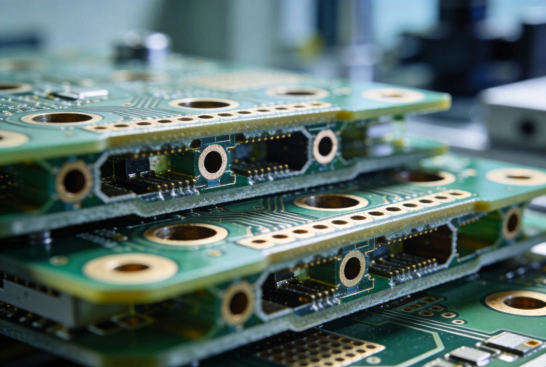
Microvias represent a fundamental shift from traditional through-hole vias, offering dramatically smaller dimensions and improved electrical performance. While standard through-hole vias might measure 300-400 microns in diameter, microvias typically range from 50-150 microns. This size reduction enables far higher routing density, allowing more signal traces in less board real estate. The mechanical aspect matters too—smaller vias require less board space and create less disruption to signal layers below.
The manufacturing processes behind microvias differ significantly from standard via formation. Laser ablation has become the dominant technology for creating microvias, as it can precisely remove dielectric material without damaging underlying copper layers. The laser creates a tapered via barrel that facilitates plating and improves current flow compared to the vertical walls of mechanically drilled vias. Alternative methods include plasma etching for certain dielectric materials and photolithographic processes for very fine features, though laser ablation remains the workhorse of high-volume microvia production.
Microvia aspect ratio—the ratio of depth to diameter—constrains manufacturing capability and directly affects cost. Industry standard limits hover around 0.8:1 to 1:1, meaning a 100-micron diameter via can be reliably formed to about 100 microns deep. Some advanced manufacturers push toward 1.5:1 or even 2:1 ratios, but these capabilities come at premium pricing and reduced yield. Design rules that respect aspect ratio limitations prevent manufacturing failures and unnecessary cost escalation.
Blind Vias connect an outer layer to one or more inner layers without penetrating the entire board stackup. These structures appear in virtually every smartphone and tablet, where they enable the dense routing required by processors and memory packages. Blind Vias are formed before the final board lamination, requiring careful registration between Sequential Lamination steps. The number of Sequential Lamination cycles directly impacts manufacturing complexity and cost, making stackup planning a critical early-stage design activity.
Buried vias exist entirely within inner layers, invisible from the outer surfaces of the board. These vias enable routing flexibility that would be impossible with only surface-visible features, allowing signals to transition between inner layers without consuming surface real estate. Buried via formation requires similar sequential lamination techniques to blind vias, with inner-layer vias being drilled and plated before outer layers are added to the stackup.
stacked microvias represent the most advanced configuration, where multiple microvia structures are directly stacked on top of each other to create vertical interconnects spanning several layers. This approach maximizes routing density by eliminating the horizontal spacing normally required between separate via structures. However, stacked microvias demand precise manufacturing control and are typically reserved for the most space-critical applications. Reliability concerns around Thermal Cycling have limited widespread adoption, though newer filling technologies and materials continue to improve performance.
Via-in-pad places vias directly within component pads rather than routing traces to vias located adjacent to pads. This approach eliminates the inductance and resistance introduced by extended trace paths, critical for high-speed signals and power distribution networks. In power delivery applications, via-in-pad structures dramatically reduce impedance by connecting component pads directly to underlying power planes. For high-speed digital signals, the shortened current return path minimizes loop inductance and reduces electromagnetic interference.
The manufacturing challenge with via-in-pad stems from solder compatibility. During assembly, molten solder can wick down through the via barrel, creating insufficient solder for a reliable joint. Alternatively, outgassing from plating chemicals within the via can create voids in the solder joint. These issues have traditionally limited via-in-pad adoption to specialized applications, but modern filling and capping technologies have expanded its utility across a broader range of products.
Thermal Management benefits make via-in-pad particularly valuable for power components. Components handling significant current generate heat that must dissipate efficiently to prevent premature failure. Via-in-pad structures provide direct thermal paths from the component to inner plane layers, which can spread heat across larger areas or connect to external heatsinks. This thermal advantage explains why virtually all modern CPUs and power management ICs rely on thermal via-in-pad configurations.
Non-conductive fill employs dielectric materials to plug the via barrel after plating. This method prevents solder wicking effectively but creates a void-prone filling that may affect thermal performance. Non-conductive fills work well for signal vias where thermal conductivity is less critical, and the lower cost compared to conductive alternatives makes this the default choice for many applications. Material Selection matters—some fills have thermal expansion characteristics that stress surrounding copper structures during Thermal Cycling.
Conductive fill uses copper or silver-filled epoxies to completely fill the via barrel after plating. Conductive fills provide superior thermal conductivity and electrical performance, essential for high-power applications. The trade-off comes in cost and processing complexity, as conductive filling requires additional steps and more stringent Quality Control. Boards using conductive fills command a premium that may not be justified for lower-power applications where non-conductive fills perform adequately.
Via capping creates a planar surface over the plated through-hole without completely filling the barrel. This approach uses copper or conductive paste to create a cap that prevents solder penetration while maintaining some thermal and electrical benefits of the original via structure. Capping works well for Thermal Vias where the primary concern is solder flow management, and the process is less expensive than full conductive filling. However, capping creates an asymmetric fill that may not be suitable for all applications.
Design Guidelines for Via-in-Pad SuccessPad size planning for via-in-pad structures must account for the via capture pad, the component pad itself, and any Solder Mask clearance requirements. A typical BGA pad might measure 0.4mm diameter, leaving limited room for via placement. Capture pad sizes generally range from 0.2mm to 0.5mm larger than the original pad to provide adequate plating tolerance. Clearance between adjacent capture pads determines minimum pitch and directly constrains component placement density.
Solder Mask design for via-in-pad requires careful attention to prevent solder from migrating onto unintended areas. Non-solder-mask-defined (NSMD) pads where the solder mask defines the copper pad perimeter offer better control over solder joint geometry but require more precise capture pad spacing. Solder-mask-defined (SMD) pads where the mask covers pad edges provide stronger mechanical attachment but can stress small pads during thermal cycling. Most manufacturers have preferred approaches based on their specific processes and can advise on optimal pad definitions.
Thermal relief connections may still be appropriate for via-in-pad designs in certain circumstances, balancing direct thermal paths against manufacturing tolerances. Some designers use partial relief patterns that provide partial connection while reducing thermal mass. Others implement capture pad designs that include stress-relief slots or reduced copper width sections. These approaches require validation through thermal cycling testing before production implementation.
X-ray inspection has become essential for via-in-pad quality verification, as internal defects cannot be detected through visual inspection alone. Cross-sectional analysis provides definitive information about fill quality and void content but destroys the inspected samples, limiting its use to qualification and periodic sampling. Automated X-ray systems can scan production boards and identify voids, cracks, or delamination issues without destroying the board, enabling 100% inspection for critical applications.
Cross-section analysis, while destructive, provides the most detailed quality information for new designs or process changes. This technique reveals fill completeness, plating quality, and interface adhesion that impact long-term reliability. Qualification testing typically includes cross-section samples from each new stackup configuration, with periodic sampling throughout production runs to verify process stability. The cost of cross-section testing is justified by the field failures it prevents.
Thermal cycling testing validates via-in-pad reliability under the temperature extremes expected in actual service. Military and automotive applications typically require hundreds or thousands of cycles between temperature extremes, with electrical continuity verification after each test interval. Failure modes include fill cracking, interface delamination, and solder joint fatigue—issues that cross-section and X-ray inspection can identify before shipping to customers.
Via-in-pad and microvia technologies add significant cost compared to standard PCB processes, with microvia costs scaling roughly inversely with diameter—halving the via size roughly doubles the cost per via. Sequential lamination steps multiply costs further, as each additional lamination cycle adds processing time and introduces yield loss. Design optimization that minimizes layer count and via complexity directly impacts manufacturing cost.
Volume economics favor HDI technologies when production quantities justify process setup costs. Prototype and low-volume runs often carry disproportionately high per-board costs because setup expenses amortize across fewer units. Design-for-manufacturing reviews that identify opportunities to use standard processes rather than advanced HDI features can significantly reduce prototype costs. Production scaling typically follows learning curves that reduce per-unit costs as volumes increase.
Alternative approaches sometimes achieve similar density without Microvia Technology. High-density trace routing, creative layer usage, and strategic component placement can often approach HDI density at lower cost. The decision between traditional high-layer-count boards versus lower-layer-count boards with microvias involves trade-offs between routing flexibility, signal integrity, Thermal Management, and manufacturing cost that vary by application.
Smartphones and mobile devices represent the highest-volume application for advanced Hdi Technology, where microvia counts per board often number in the thousands. The relentless pressure to reduce size while adding features has pushed mobile manufacturers to adopt any-layout (ALIVH) and other advanced HDI structures that maximize routing density. Manufacturing volumes in this segment justify massive capital investment in cutting-edge equipment, and many HDI innovations first deployed in smartphones later migrate to other applications.
Medical implants increasingly rely on Hdi Technology to pack sophisticated electronics into packages small enough for implantation. Hearing aids, pacemakers, and neurostimulators use flexible and rigid-flex HDI constructions that conform to body contours while housing complex signal processing circuitry. Biocompatible materials and extreme reliability requirements push these applications toward the most advanced manufacturing capabilities available.
Automotive electronics adoption of HDI technology continues accelerating as vehicles add more electronic content. Advanced driver assistance systems, infotainment, and engine control modules require reliable performance across extreme temperature ranges and prolonged service lives. Automotive qualification requirements often exceed those of consumer electronics, demanding more thorough testing and documentation of manufacturing processes.
Embedded active components represent the next frontier in PCB miniaturization, with transistors and other active devices built directly into the board substrate rather than mounted on its surface. This approach eliminates component footprints entirely, though manufacturing challenges around thermal management and device integration remain substantial. Several manufacturers currently offer limited embedded component capabilities, with broader adoption expected as processes mature.
Substrate-like PCB (SLP) technology borrows manufacturing techniques from semiconductor packaging to create finer features than traditional PCB processes allow. Panel-level packaging applies semiconductor fabrication methods to larger substrates, potentially reducing costs for high-volume applications while enabling unprecedented routing density. These hybrid approaches blur traditional boundaries between IC packaging and Pcb Manufacturing.
Advanced materials including low-loss dielectrics, high-thermal-conductivity substrates, and embedded capacitance materials enable performance improvements beyond simple density gains. These material innovations often accompany microvia and via-in-pad technologies to address thermal management, signal integrity, and reliability requirements that increasingly constrain system design. Material Selection decisions made early in the design process significantly impact achievable performance.
Via-in-pad and microvia technologies form the foundation of modern HDI solutions, enabling the miniaturization that today's electronic products demand. While these approaches introduce manufacturing complexity and cost premiums, their benefits—improved electrical performance, enhanced thermal management, and dramatically increased routing density—justify adoption in demanding applications. Understanding the trade-offs involved in via type selection, filling methods, and stackup planning empowers engineers to make informed design decisions that balance performance against manufacturing reality.
Successful implementation of advanced HDI features requires early engagement with manufacturing partners who can advise on capability limitations and process optimization. Design rule development that reflects actual manufacturing capabilities prevents costly revisions and ensures producible designs. As electronic products continue evolving toward greater functionality in smaller packages, HDI expertise becomes an increasingly valuable competitive advantage.
Whether designing the next generation of mobile devices, medical implants, or automotive control systems, the principles covered here provide a framework for evaluating and implementing via-in-pad and microvia technologies. The specific implementation details will continue evolving as manufacturing capabilities advance, but the fundamental trade-offs between density, cost, reliability, and manufacturability will remain central to HDI design decisions.
What is the main advantage of microvias over traditional through-hole vias?
Microvias offer significantly smaller dimensions—typically 50-150 microns versus 300-400 microns for standard vias—enabling far higher routing density. Their tapered geometry from laser formation also provides better plating quality and electrical performance compared to mechanically drilled vertical vias.
How does via-in-pad improve thermal management?
Via-in-pad creates direct thermal paths from component pads to inner plane layers, bypassing the extended paths required when vias are placed adjacent to pads. This direct connection efficiently transfers heat away from components, reducing junction temperatures and improving reliability for power-dissipating parts.
What filling method should I choose for thermal via-in-pad structures?
Conductive filling provides the best thermal conductivity for high-power applications but at higher cost. Non-conductive filling works adequately for lower-power Thermal Vias where cost optimization is important. Via capping offers a middle ground with reasonable thermal performance at moderate cost.
What limits microvia aspect ratio in manufacturing?
Manufacturing reliability limits microvia aspect ratio to roughly 1:1 in most facilities, meaning a 100-micron diameter via can be formed about 100 microns deep. Advanced manufacturers may achieve 1.5:1 or higher ratios, but these capabilities come at premium pricing and reduced yields.
Why do stacked microvias face reliability concerns?
Stacked microvias create structures with multiple interfaces between different material systems. Thermal expansion mismatches during temperature cycling can cause stress concentrations at these interfaces, potentially leading to cracking or delamination. Modern filling technologies and improved materials continue addressing these concerns.
Understanding Metal Core PCBs (MCPCB) for Superior Thermal ManagementJuly/13/2026
End-to-End Industrial PCB Solutions: From Design to DeliveryJuly/08/2026
Custom Industrial PCB Solutions for the Automotive SectorMay/27/2026

How to Find the Right Partner for Your Custom Industrial PCB SolutionsJuly/24/2026
Unlocking Performance with High-Layer Count Industrial PCB SolutionsJune/15/2026

Tailored Industrial PCB Solutions for Medical Device ManufacturersJune/12/2026
Design Guidelines for Durable Flex PCB Solutions in Dynamic ApplicationsJuly/10/2026
Manufacturing Challenges in 20+ Layer Industrial PCB SolutionsJuly/09/2026