Open Nav


Every material expands when heated and contracts when cooled. This fundamental physical behavior, quantified by the coefficient of thermal expansion (CTE), creates persistent challenges in electronic assembly. As circuit boards cycle through temperature during manufacturing, testing, and field operation, mismatched expansion rates between different materials generate stress that accumulates into failures over time. Understanding CTE and its implications for material selection determines whether electronic products survive or fail in demanding applications.
This article explores the science behind thermal expansion mismatch, examines how CTE affects various aspects of Pcb Design and manufacturing, and provides practical guidance for selecting materials that work together reliably. Whether you're designing for automotive under-hood environments, aerospace applications, or industrial equipment, managing CTE effects ensures your assemblies endure throughout their intended service life.
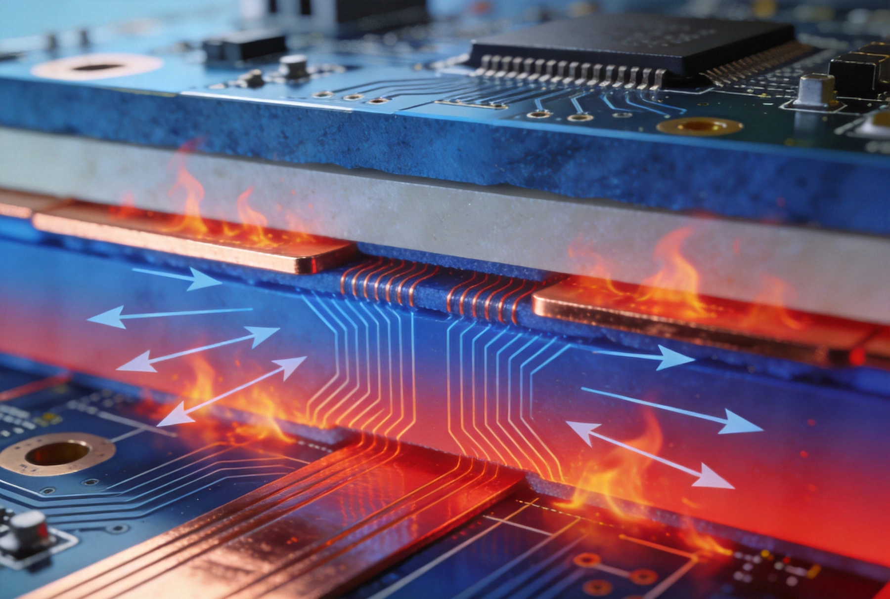
The coefficient of thermal expansion describes how much a material changes dimension per degree of temperature change. CTE is typically expressed in parts per million per degree Celsius (ppm/°C), indicating the fractional expansion per unit temperature increase. A material with a CTE of 15 ppm/°C expands by 15 millionths of its length for each degree Celsius temperature rise.
Different materials exhibit vastly different CTE values. Copper, the primary conductor in PCBs, has a CTE of approximately 17 ppm/°C in the plane of the foil and higher through its thickness. FR-4 epoxy-glass laminate, the most common Pcb Substrate, ranges from 12-16 ppm/°C in-plane depending on glass weave content. Ceramic materials used in some electronic packages display CTEs around 6 ppm/°C, while typical lead-free solder alloys approach 20-25 ppm/°C.
Materials expand differently in different directions, particularly composites and crystalline materials. Copper Foil expands fairly uniformly in all directions, though rolled copper shows slight anisotropy. FR-4 exhibits different CTE in the X-Y plane (in-plane) versus the Z-axis (through thickness), with the through-plane CTE being significantly higher—sometimes 3-5 times the in-plane value. This directional behavior affects how different materials interact in multilayer constructions.
Understanding CTE in three dimensions becomes crucial for BGA packages and other area-array components. The silicon die inside a BGA has a CTE around 3 ppm/°C, while the Pcb Substrate may expand at 15-20 ppm/°C. This mismatch creates shear stress on solder joints during temperature changes that can crack connections over thermal cycles. Package design must account for this differential to ensure reliable interconnection.
Multilayer PCBs contain copper planes, dielectric layers, and traces arranged in stacks that constrain each other's thermal expansion. The copper in planes and traces tries to expand at its native CTE, but the surrounding dielectric material resists this expansion. This constraint creates internal stresses that build up during temperature changes and can cause various failure modes including plated-via barrel cracking, trace lifting, and Delamination between layers.
Plated-through holes face particularly challenging conditions because they traverse the entire board thickness, connecting layers with potentially different in-plane expansion characteristics. During thermal cycling, the barrel of the via experiences shear stress as the surrounding dielectric expands and contracts differently than the copper barrel. This cyclic stress eventually fatigues the copper plating, creating cracks that may cause intermittent or complete electrical opens.
The most critical CTE mismatch in electronic assembly occurs between components and boards. Surface mount components made of ceramic materials have CTEs around 6 ppm/°C, while organic PCB substrates typically expand at 15-20 ppm/°C. This fivefold difference means that a temperature change of 100°C produces five times more expansion in the board than in the component body, with the solder joints absorbing this differential.
Solder joints must accommodate this mismatch through deformation. The shear strain in the joint depends on the CTE difference, the distance from the component neutral point, and the joint height. Larger components and packages with higher lead counts experience greater thermal strain because their corners move further relative to the board surface. BGA packages, while avoiding lead-related issues, face similar solder joint stress from CTE mismatch.
FR-4 remains the workhorse substrate for most PCB applications due to its balanced properties and cost effectiveness. Standard FR-4 CTE in the X-Y plane typically ranges from 13-16 ppm/°C, varying with glass weave style, resin content, and laminate construction. The glass reinforcement constrains the epoxy resin, reducing in-plane CTE compared to unreinforced epoxy which might reach 50-70 ppm/°C.
For lead-free assembly processes that require higher reflow temperatures, manufacturers have developed enhanced FR-4 grades with improved thermal stability. These materials maintain glass transition temperatures (Tg) above 170°C compared to standard grades around 130-140°C. Higher Tg materials experience less softening during elevated temperature exposure, reducing stress buildup during thermal cycling. However, CTE values for these materials remain similar to standard FR-4.
Polyimide-based laminates offer superior thermal performance for demanding applications. With Tg values exceeding 250°C, polyimide materials resist softening at temperatures that degrade epoxy resins. Their CTE values typically range from 12-16 ppm/°C in-plane, similar to FR-4, but their thermal stability allows exposure to multiple high-temperature assembly cycles without property degradation.
The primary drawback of polyimide is cost—typically 3-5 times the price of equivalent FR-4 laminates. Polyimide also absorbs moisture more readily than epoxy, requiring special handling to prevent moisture-related Delamination during assembly. For applications where thermal cycling endurance or high-temperature operation justifies the expense, polyimide provides reliable performance that standard materials cannot match.
Bismaleimide triazine (BT) epoxy laminates offer another high-performance option with different property trade-offs than polyimide. BT resins provide good thermal stability with lower moisture absorption than polyimide. Their CTE characteristics suit applications involving semiconductor packaging where they interface with chip-scale packages and other advanced component technologies.
Other resin systems including cyanate ester and hydrocarbon blends offer specific advantages for niche applications. Cyanate ester provides excellent electrical properties with low dielectric loss at high frequencies. Hydrocarbon resin materials bridge the gap between FR-4 and specialized high-performance laminates, offering improved thermal performance at moderate cost increases for applications requiring better thermal cycling resistance.
Metal core PCBs insert aluminum or copper cores between dielectric layers to dramatically improve Thermal Conductivity. These constructions serve applications where heat spreading from hot components is essential. The metal core constrains in-plane thermal expansion of the Dielectric Layer, reducing board-level CTE mismatch with components.
Insulated Metal Substrate (IMS) constructions place a thin dielectric directly on a metal base, creating efficient heat transfer paths while maintaining electrical isolation. The metal base expands at its native CTE (approximately 23 ppm/°C for aluminum), which can either help or hurt component stress depending on the specific application. Careful thermal modeling helps predict stress levels in metal core assemblies.
Strategic component placement reduces CTE-related stress by minimizing differential movement. Placing components with similar CTE sensitivity together enables uniform Thermal Management. Grouping BGAs and large QFP packages away from smaller passive components allows targeted thermal relief without compromising the assembly of easier-to-assemble parts.
The location of components relative to board neutral points affects stress levels at corners and edges. Components positioned near the board center experience less thermal movement relative to each other than components at opposite corners. For assemblies with multiple large packages, distributing stress across the board rather than concentrating it in one area extends fatigue life.
Copper trace routing affects local CTE behavior through the constraint that traces impose on substrate expansion. Heavy copper planes and traces constrain local dielectric expansion, creating stress concentrations at trace-to-pad transitions. These concentrations can initiate cracks that propagate under thermal cycling, particularly in plated through-holes adjacent to heavy copper features.
Thermal relief connections between plane copper and via barrels reduce thermal stress concentrations by allowing more flexible current paths. The narrow neck of thermal relief arms provides compliance that absorbs differential expansion between the plane and the plating on the via barrel. Standard thermal relief patterns specify arm widths and spacing that provide adequate compliance while maintaining electrical connectivity.
Lead-free solder assembly exposes boards to peak temperatures of 245-260°C, significantly higher than traditional tin-lead processes. These elevated temperatures create larger thermal excursions from the stress-free state than lead-based assembly, potentially causing more damage during each assembly cycle. Boards that survive multiple lead-free reflow passes accumulate more stress damage than boards processed through tin-lead profiles.
Optimizing reflow thermal profiles reduces CTE-related stress without compromising solder joint quality. The time above liquidus and peak temperature directly affect residual stress in the assembly. Slower heating and cooling rates reduce thermal gradients through the board thickness, decreasing differential expansion between layers. Soak zones that equilibrate temperature before peak heating also reduce stress buildup.
Rework operations introduce additional thermal stress cycles that may damage boards already stressed from assembly. Localized heating for component removal and replacement creates temperature gradients that generate stress even when the overall board temperature remains moderate. Repeated rework can accumulate damage to the point where delamination or trace damage occurs.
Hot air rework stations with precise temperature control minimize thermal impact during repair. Preheating the entire board to moderate temperatures (80-100°C) reduces temperature gradients during localized rework. Underfill removal before BGA rework prevents thermal shock to adjacent components. These practices extend board life through multiple rework cycles.
Thermal cycling testing accelerates the fatigue damage that occurs in field service, revealing CTE-related weaknesses before production deployment. Standard test profiles specify temperature extremes, dwell times, and cycle counts that represent expected field conditions. IPC-9701 defines thermal cycling tests specifically for surface mount solder joint reliability, with profiles ranging from 0°C to 100°C for commercial applications up to -55°C to 125°C for military-grade products.
Accelerated testing must balance severity against introducing failure modes that wouldn't occur under real-world conditions. Extremely fast temperature changes create thermal gradients that exceed those in actual service, potentially causing failures that wouldn't happen in normal operation. Industry-standard test methods have been refined through decades of correlation with field performance to ensure relevant results.
When thermal cycling reveals failures, accurate diagnosis identifies the root cause so design improvements address the actual weakness. Cross-sectional analysis of failed joints reveals crack locations and propagation patterns that indicate whether stress concentration occurred in the solder, at the component interface, or at the board metallization. X-ray Inspection finds voids and defects that predispose joints to Thermal Fatigue.
Root cause determination distinguishes CTE mismatch failures from other thermal damage mechanisms. Poor solder wetting produces failure at interfaces that differ from fatigue cracking. Pad cratering creates failures in the board material rather than the solder joint. Accurate diagnosis prevents unnecessary design changes that address symptoms rather than causes.
Material selection should start with application requirements that define thermal environment severity. Consumer electronics operating in controlled environments may tolerate standard FR-4 with conventional assembly processes. Automotive under-hood applications requiring extended temperature range benefit from high-Tg or polyimide materials. Aerospace and defense applications typically mandate polyimide or specialized laminates meeting specific military specifications.
Expected service life directly affects material selection because CTE stress damage accumulates over time. Products designed for five-year service life can accept materials and stress levels that wouldn't be acceptable for fifteen-year applications. Matching material performance to application life requirements optimizes cost without sacrificing reliability.
Laminate manufacturers provide detailed technical data sheets that enable informed material selection. CTE values, Tg, and thermal decomposition temperatures define the thermal operating envelope. Processing guidelines specify drilling, plating, and lamination parameters that achieve optimal results with each material. Early engagement with suppliers prevents specification of materials that don't support the intended manufacturing process.
Many suppliers offer design-in support that helps optimize material selection for specific applications. Their engineering teams have experience across thousands of applications and can recommend materials that others have successfully used for similar requirements. This expertise complements internal engineering judgment to produce optimal designs.
Development continues on new Pcb Materials that better manage CTE effects while meeting other requirements like high-frequency performance and environmental sustainability. Low-CTE fillers added to standard resins reduce in-plane expansion, potentially enabling FR-4 cost structures with improved thermal cycling performance. Nanocomposite materials incorporating carbon nanotubes or graphene promise property improvements that current material systems cannot achieve.
Additive manufacturing approaches for electronics may eventually circumvent some CTE challenges by enabling materials integration impossible with traditional lamination. Embedding components within the board structure rather than mounting them on surfaces reduces differential expansion effects. While these technologies remain developmental, monitoring their progress prepares designers for future opportunities to address CTE challenges through novel approaches.
Coefficient of thermal expansion fundamentally affects Industrial Pcb material selection and assembly reliability. The mismatch between expansion rates of different materials creates stress that accumulates into failures over thermal cycles. Understanding CTE mechanics, material property relationships, and design strategies enables engineers to select appropriate materials and design assemblies that endure their intended service life.
Material selection balances thermal performance requirements against cost constraints. Standard FR-4 serves many applications adequately when design practices address CTE effects, while demanding applications justify premium materials that provide superior thermal cycling endurance. Working closely with material suppliers and assembly partners ensures that material selection decisions are informed by both theoretical understanding and practical manufacturing experience.
As electronic products continue pushing into more demanding thermal environments, CTE management becomes increasingly critical. Electric vehicle Power Electronics, renewable energy systems, and advanced computing applications all create thermal challenges that require careful material selection and design optimization. Building expertise in CTE effects prepares engineering teams to address these emerging requirements successfully.
The Rise of Halogen-Free Industrial PCB Materials: Benefits and Trade-offsAugust/06/2026
A Comprehensive Guide to High-Tg Materials for Industrial PCBsMay/27/2026
How to Select Industrial PCB Materials for High-Voltage ApplicationsSeptember/07/2026
FR-4 vs. Polyimide: Choosing the Right Industrial PCB MaterialsJuly/02/2026
A Comprehensive Guide to High-Tg Materials for Industrial PCBsJune/05/2026
Copper Weight Matters: Optimizing Industrial PCB Materials for Power ElectronicsSeptember/23/2026

How Automation is Revolutionizing Industrial PCB Production in 2026September/02/2026
Essential Rules for Industrial PCB DesignJune/08/2026