

The surface finish applied to bare copper traces determines how effectively components solder to your board. Every millimeter of trace geometry requires protection from oxidation while maintaining solderability throughout assembly and product lifetime. Choosing the appropriate surface finish affects manufacturing yields, field reliability, and total product cost in ways that extend far beyond the initial finishing expense. Industrial applications place particular demands on surface finish selection, where failure consequences exceed consumer electronics stakes.
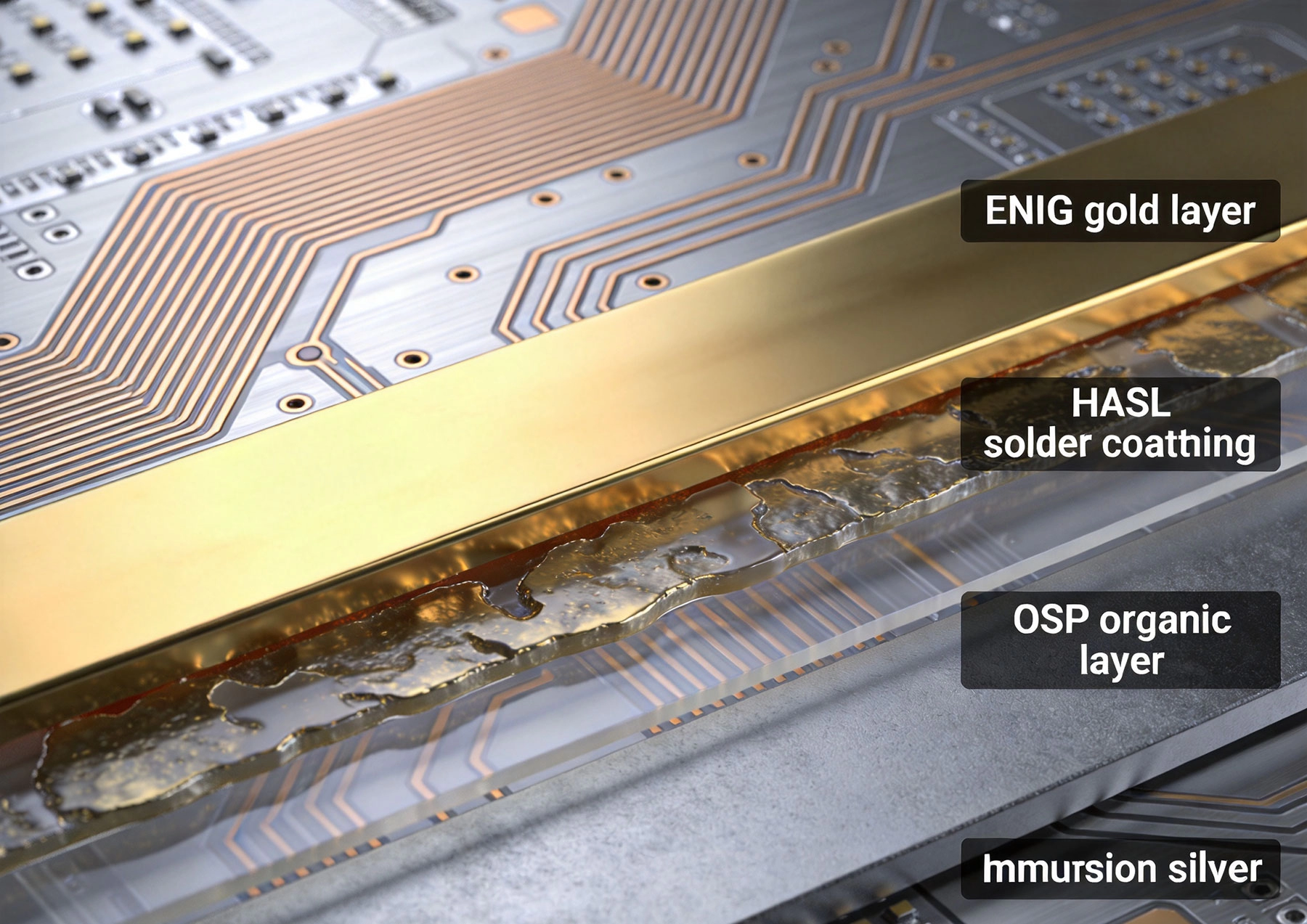
Copper oxidizes rapidly when exposed to air, forming copper oxide and copper carbonate layers that prevent reliable solder wetting. Surface finishes serve dual purposes: protecting copper during storage and handling while providing solderable surfaces that form reliable metallurgical bonds with component leads.
The finish you select influences multiple fabrication parameters. Shelf life determines how long boards remain solderable after receipt. Surface planarity affects placement accuracy for fine-pitch components. Solderability window controls assembly process flexibility. Each characteristic impacts Manufacturing Efficiency and product reliability differently depending on your application requirements.
Industrial and automotive applications demand finishes that withstand harsh operating conditions—temperature extremes, vibration, humidity—while maintaining electrical integrity over extended product lifetimes measured in decades. Consumer applications prioritize cost efficiency and high-volume assembly compatibility. The same finish rarely serves both applications optimally.
Surface finishes deposit thin metallic or organic layers over copper surfaces. Thickness ranges from fractions of a micron for organic preservatives to 3-6 microns for electrolytic nickel gold. Thickness determines both protection effectiveness and potential complications like bridging in fine-pitch applications.
Different deposition methods produce finishes with varying uniformity and coverage characteristics. Electroless processes deposit uniformly regardless of geometry, while electrolytic processes may deposit unevenly on complex board features. Understanding deposition methods guides selection for specific board geometries.
HASL represents the traditional PCB surface finish, coating copper with solder through a hot air leveling process. Molten solder adheres to exposed copper while hot air knives blade excess solder, leaving relatively smooth surfaces.
Traditional tin-lead HASL provides excellent solderability and long shelf life—typically two years without special storage requirements. The finish tolerates multiple high-temperature assembly cycles without degrading, suitable for boards requiring rework or multiple assembly stages.
Surface planarity varies with board geometry. Large pads level consistently while smaller pads or dense area arrays may exhibit uneven coverage or dewetted spots. Hole diameter reduction from solder in plated through-holes sometimes requires tighter control for press-fit connectors.
RoHS compliance drove adoption of lead-free HASL alternatives using tin-copper, tin-nickel, or other alloy compositions. Lead-free alternatives generally provide adequate performance but present distinct challenges compared to traditional tin-lead.
Higher melting temperatures of lead-free alloys require adjusted reflow profiles that may stress temperature-sensitive components. Tin whisker formation concerns exist for some lead-free compositions, though modern alloys incorporate additives minimizing whisker risks. Cost premiums for lead-free HASL vary with tin commodity prices.
HASL suits applications with generous pad geometries—typically components with pitch exceeding 0.5mm. Through-hole technology and larger surface mount packages level well and solder reliably. The finish tolerates surface variations that would cause problems for fine-pitch components.
Budget-conscious projects benefit from HASL cost advantages over premium finishes. High-volume consumer products often accept HASL trade-offs in surface planarity for manufacturing cost savings. The finish provides reliable solderability when application geometry accommodates its characteristics.
ENIG deposits a nickel barrier layer over copper followed by a thin gold flash. This two-layer system provides excellent surface planarity and corrosion protection for demanding applications.
Surface planarity approaching absolute flatness makes ENIG ideal for fine-pitch components like BGA, QFN, and packages with 0.4mm pitch or finer. Placement equipment achieves accurate component positioning because pads present uniform reference surfaces without height variations.
The nickel barrier prevents copper diffusion into solder joints, maintaining metallurgical stability over extended Thermal Cycling. Gold dissolves rapidly into solder during assembly, exposing fresh nickel surfaces that wet reliably. This predictable dissolution simplifies process control compared to finishes requiring careful Thermal Management.
ENIG processing requires tight control to prevent nickel corrosion—commonly called black pad. Improper ENIG bath chemistry or contamination creates nickel surfaces that resist solder wetting, causing weak joints and field failures.
Reputable manufacturers implement rigorous process controls preventing black pad formation. Ipc Standards specify acceptable nickel and gold thickness ranges that minimize corrosion risk. Understanding your manufacturer's ENIG process capabilities and quality systems matters more than finish selection alone.
RF and microwave applications often favor ENIG due to Controlled Impedance characteristics. The gold surface provides stable, low-resistance contacts suitable for high-frequency signals. However, Skin Effect considerations at very high frequencies require attention to gold thickness and its slight resistance contribution.
OSP applies thin organic coatings that protect copper surfaces temporarily. These water-based treatments conformally coat copper, preventing oxidation while remaining solderable when flux activates the coating during assembly.
OSP provides excellent surface planarity approaching ENIG flatness at lower cost. The thin organic layer adds negligible thickness, maintaining fine-pitch geometry accurately. Environmentally friendly water-based chemistry avoids heavy metal concerns associated with ENIG and HASL processes.
OSP works well with lead-free solders, avoiding HASL process complications with high-temperature assembly profiles. Multiple thermal cycles degrade OSP protection, so boards with extended assembly processes require careful handling or alternative finishes.
Shelf life remains shorter than metallic finishes—typically six months to one year depending on storage conditions. Humidity and temperature accelerate degradation, requiring sealed packaging and controlled storage environments. Boards approaching shelf life limits may exhibit dewetting during assembly.
OSP cannot withstand multiple assembly cycles as well as metallic finishes. Rework operations risk damaging OSP protection on adjacent components, potentially requiring touch-up with alternative processes. The finish also proves unsuitable for pressed contacts or wire bonding applications where gold or nickel surfaces are required.
OSP suits high-volume assembly with quick-turn requirements where boards flow directly from fabrication to assembly. Single-pass assembly processes with controlled environments maximize OSP benefits. The finish provides excellent cost-performance balance for consumer products without extended storage or multi-cycle assembly requirements.
Immersion silver deposits thin silver layers directly over copper through displacement plating. The process produces bright, solderable surfaces with excellent planarity and cost-performance characteristics.
Silver provides excellent solderability with lower contact resistance than OSP or HASL surfaces. The finish accommodates fine-pitch components with surface planarity comparable to ENIG. Deposition thickness typically ranges from 3-8 microns—thin enough to avoid bridging concerns while providing adequate protection.
Shelf life exceeds OSP—approximately one year with proper storage—though silver surfaces tarnish when exposed to sulfur-containing atmospheres. Hermetic sealing or controlled storage extends usability, while uncontrolled environments may see surface degradation within months.
Silver migration—dendritic growth between adjacent conductors under bias—historically concerned designers. Modern formulations incorporating inhibitors and proper design spacing mitigate migration risks for most applications. Designs with fine spacing and high voltage differences may warrant alternative finishes or protective coatings.
Immersion silver serves applications requiring ENIG-quality planarity without associated costs. LED lighting, Automotive Electronics, and industrial controls frequently employ immersion silver for balanced performance and pricing. The finish accommodates both lead-free and traditional solders, providing manufacturing flexibility.
Immersion tin deposits tin directly over copper through displacement reactions. The finish provides good solderability with moderate shelf life and cost positioning between OSP and premium finishes.
Immersion tin produces uniform coatings suitable for fine-pitch applications with surface planarity approaching ENIG quality. The finish maintains solderability through multiple assembly cycles better than OSP, tolerating limited rework without complete surface preparation.
Tin surfaces remain vulnerable to oxidation and tin whisker formation despite industry efforts to control these phenomena. Storage requirements and shelf life considerations apply similarly to other non-barrier finishes. Intermetallic compound growth between tin and copper may affect long-term solderability if boards exceed storage limits.
Immersion tin suits applications where nickel-containing finishes present concerns—particularly medical devices where nickel sensitivity affects end users. The finish avoids nickel entirely while providing solderability approaching ENIG quality. Cost positioning makes immersion tin attractive for cost-sensitive industrial applications.
Demanding applications requiring gold thickness beyond ENIG flash capabilities need electrolytic hard gold plating. Specialized finishes also address particular requirements like aluminum wire bonding or high-wear environments.
Electrolytic hard gold deposits thicker gold layers—typically 15-30 microinches minimum—over nickel underlayers. This thick gold provides wear resistance suitable for edge connectors, Test Points, and applications requiring repeated mating cycles.
The thick gold maintains contact integrity where mechanical wear would quickly degrade thinner finishes. Process control proves simpler than ENIG because gold thickness correlates directly with plating current and time. Edge connectors require dedicated rack or strip plating processes creating design constraints.
Medical implants, aerospace electronics, and specialized sensors often require aluminum wire bonding to PCB surfaces. Gold-over-nickel finishes provide ideal surfaces for ultrasonic wire bonding, with nickel providing adhesion and gold enabling reliable bond formation.
Bond pull strength and wire bond reliability depend critically on proper gold and nickel thickness specifications. Ipc Standards specify minimum requirements for wire bonding applications. Close coordination between design requirements and manufacturer capabilities ensures proper finish implementation.
Different industrial sectors present distinct finish requirements based on operating environments and reliability expectations.
Automotive applications require finishes surviving temperature cycling from -40°C to +125°C or higher, vibration, and humidity exposure. ENIG provides proven reliability for critical safety systems where joint failure carries severe consequences. Iatf 16949 quality management requirements ensure process control consistency supporting automotive reliability.
Factory automation and industrial equipment electronics prioritize long-term availability and moderate cost. Immersion silver or quality HASL provide adequate reliability at attractive price points. These applications often accept trade-offs between premium finish performance and manufacturing cost efficiency.
Medical electronics demand finishes supporting reliability requirements spanning product lifetime—sometimes twenty years or longer. ENIG remains prevalent despite cost premiums due to proven long-term stability. Nickel-free finishes like immersion silver address biocompatibility concerns for devices contacting patients.
Solar inverters, motor drives, and power conversion equipment operate at elevated temperatures challenging many finish types. ENIG provides stable performance under Thermal Cycling while HASL tolerates high-temperature operation without degradation. Application-specific thermal requirements may drive finish selection beyond general guidelines.
Surface finish costs range from under $0.01 per square inch for basic HASL to $0.05-0.10 for premium ENIG. These direct material and processing costs represent fractions of total product value but influence manufacturing yields and field reliability substantially.
Finish-related failures impose costs beyond rework and scrap. Customer returns damage brand reputation. Field service calls consume margins. Product liability claims threaten company survival. These indirect costs often exceed direct finish premiums by orders of magnitude for applications where reliability matters.
Assembly yield losses from poor solderability multiply across production volumes. A 1% yield loss on high-volume production represents substantial cumulative cost. Finish selection affects first-pass yield through solderability consistency and surface planarity impacting placement accuracy.
Optimal finish selection considers total cost across product lifecycle, not merely fabrication expense. Premium finishes commanding higher unit costs may reduce total cost when their reliability prevents more expensive field failures. Conservative selection for critical applications often proves economically rational despite apparent cost premiums.
Application-criticality drives appropriate selection. Commodity products with short service life and minimal failure consequences may accept finish trade-offs appropriate for premium applications. Matching finish capability to application requirements avoids both under-specification failures and over-specification waste.
Surface finish selection determines fundamental manufacturing success and product reliability. Each finish type presents distinct characteristics suitable for particular applications—HASL for cost-sensitive products with adequate geometry, ENIG for demanding applications requiring fine-pitch capability and long-term stability, OSP for high-volume assembly with controlled storage, and immersion silver for balanced performance and pricing.
Industrial applications warrant particular attention to finish selection. Reliability expectations exceed consumer applications, operating environments challenge finish performance, and product lifetimes extend potential failure windows. Premium finishes often prove justified despite apparent cost premiums.
Work with fabrication partners experienced in your application sector. Their expertise in finish selection and process control prevents issues arising from inappropriate specifications. Request samples when evaluating new finish applications, and validate performance through assembly process qualification before production commitment.
The minimal cost of surface finish optimization compared to failure consequences makes thorough evaluation worthwhile. Specify finishes appropriate for your application requirements, verify manufacturer capabilities through qualification testing, and maintain process controls ensuring consistent performance throughout production.
Your board fabrication quality depends on surface finish as much as any other manufacturing parameter. Invest the attention appropriate to this critical decision, and your products will perform reliably throughout their intended service lives.
Overcoming Common Defects in Industrial PCB FabricationAugust/03/2026
Advanced Techniques in Multi-Layer Industrial PCB FabricationJune/03/2026
The Role of Laser Drilling in High-Precision Industrial PCB FabricationOctober/15/2026
Predicting Lifespan: Accelerated Life Testing for Industrial PCB ReliabilityAugust/03/2026
Precision Engineering: Tolerances in High-End Industrial PCB FabricationSeptember/03/2026

How to Choose the Right Manufacturer for Industrial PCB FabricationJune/29/2026
Eco-Friendly Practices in Modern Industrial PCB FabricationSeptember/20/2026
Materials, Methods, and Industry Standards ExplainedMay/27/2026