Open Nav


Flying probe testing has revolutionized Quality Control in industrial pcb manufacturing, offering a flexible, cost-effective alternative to traditional bed-of-nails testing. As electronic products become increasingly complex and production volumes more varied, manufacturers need testing solutions that can adapt quickly without sacrificing accuracy or reliability. Flying probe testing meets this need by using movable probes to contact Test Points across the PCB surface, enabling comprehensive electrical testing without custom fixtures or extensive setup time. This technology has become indispensable for prototype testing, low-volume production, and High-mix Manufacturing environments where traditional testing methods prove impractical or cost-prohibitive.
Understanding flying probe testing's capabilities, advantages, and optimal applications helps manufacturers implement effective Quality Control strategies that balance cost, speed, and thoroughness. This comprehensive guide explores flying probe testing's role in Industrial Pcb quality control, from fundamental principles to advanced applications and best practices for maximizing its benefits in your manufacturing operations.
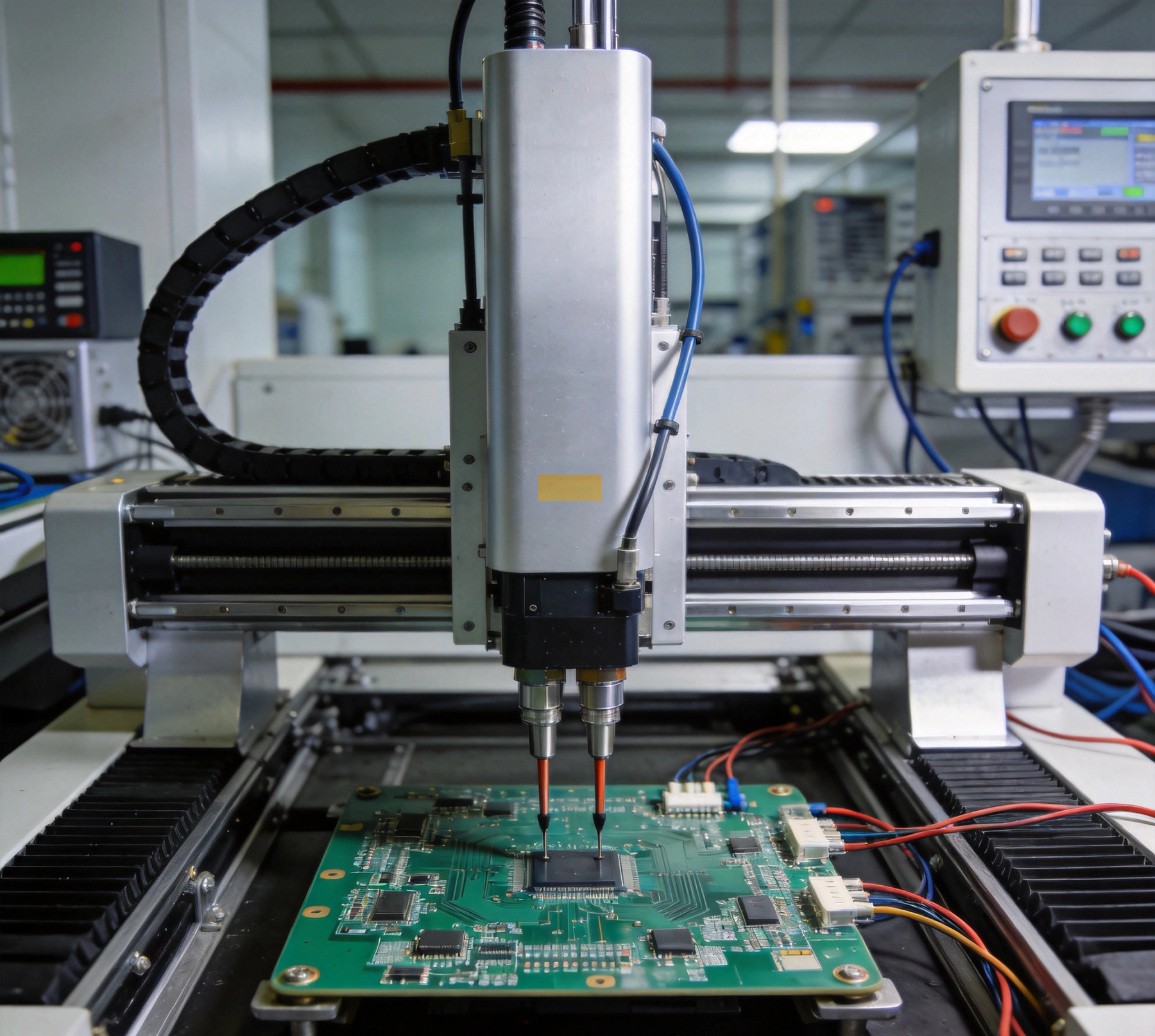
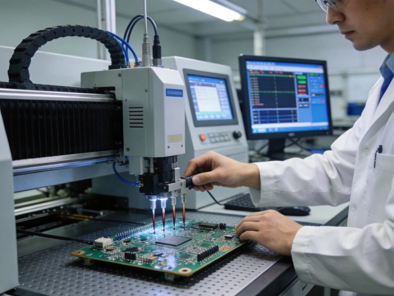
Flying probe testing represents a fundamentally different approach to Pcb Electrical Testing compared to traditional methods. The technology gets its name from the way test probes "fly" across the PCB surface under computer control, contacting designated Test Points to perform electrical measurements. Unlike bed-of-nails testers that use fixed fixtures with hundreds of spring-loaded pins making simultaneous contact, flying probe systems use a small number (typically 2-8) of precision probes that move independently to contact test points sequentially.
A typical flying probe tester consists of several key components working together:
Flying probe testers perform a comprehensive range of electrical tests:
Flying probe testing offers numerous advantages that make it attractive for many Industrial Pcb applications:
The most significant advantage of flying probe testing is the elimination of custom test fixtures. Bed-of-nails testers require expensive, complex fixtures custom-designed for each PCB type. These fixtures cost thousands to tens of thousands of dollars and take weeks to manufacture. Flying probe testing requires no fixtures at all—the probes simply move to the required test points automatically. This eliminates fixture costs, reduces lead time, and enables testing of new designs immediately after Pcb Assembly completion.
Flying probe test programs can be created quickly from CAD data, often in hours rather than the days or weeks required for fixture design and fabrication. Modern software imports Gerber files, pick-and-place data, and netlists, automatically generating test programs with minimal manual intervention. This rapid programming capability supports fast design iterations and prototype testing without bottlenecks.
When PCB designs change, updating flying probe test programs is straightforward—simply import the new CAD data and regenerate the test program. There's no need to modify or replace physical fixtures, which is particularly valuable during design verification when changes occur frequently. This flexibility supports agile development processes and rapid prototyping cycles.
Flying probe testers typically cost significantly less than comparable bed-of-nails systems. While high-end flying probe systems can cost $100,000-$200,000, basic systems start around $30,000-$50,000. This lower entry cost makes flying probe testing accessible to smaller manufacturers and prototyping facilities. The total cost of ownership remains favorable when considering the elimination of fixture costs and reduced programming time.
For production volumes up to several thousand boards per month, flying probe testing often provides the best economics. The per-board testing cost decreases as volume increases, but even at moderate volumes, flying probe testing remains cost-competitive when fixture costs are considered. This makes it ideal for prototyping, pilot production, and low-volume manufacturing where bed-of-nails testing would be uneconomical.
Flying probe systems use high-precision measurement instruments and can achieve measurement accuracy comparable to or better than bed-of-nails testers. The ability to position probes precisely enables accurate measurements at specific test points, and the sequential nature of testing allows each measurement to be optimized for accuracy rather than speed.
Flying probe testers apply controlled, minimal contact force to test points, reducing the risk of damaging delicate PCBs or components. The probes can also approach test points from optimal angles, avoiding mechanical interference that might occur with fixed fixture pins. This gentler contact is particularly important for fragile assemblies or boards with fine-pitch components.
Despite its advantages, flying probe testing has limitations that must be considered:
The sequential nature of flying probe testing means it's inherently slower than bed-of-nails testing, which makes hundreds or thousands of contacts simultaneously. Test times for complex boards can range from several minutes to over an hour per board, compared to seconds for bed-of-nails testing. This speed limitation makes flying probe testing less suitable for very high-volume production where test time directly impacts throughput.
Test probes wear over time and require regular replacement to maintain contact reliability. Probe tips can accumulate contamination, become misaligned, or lose spring force, all of which affect measurement accuracy. Implementing regular probe maintenance and replacement schedules is essential for consistent testing quality.
Flying probe testing requires physical access to test points. Components, connectors, or other obstructions can prevent probes from reaching intended test points. While vision systems help navigate around obstacles, extremely dense board layouts may have areas that are difficult to test with flying probes. Careful test point planning during design helps maximize test coverage.
The moving probes and long cable runs in flying probe systems can introduce electrical noise that affects measurement accuracy, particularly for high-impedance measurements. Shielding, proper grounding, and measurement techniques help mitigate these effects, but some measurements may still be more challenging than with bed-of-nails systems.
For very high-volume production where every second of test time impacts manufacturing throughput, flying probe testing may not provide adequate speed. In these cases, bed-of-nails testing or automated test equipment (ATE) with dedicated fixtures may be more appropriate despite the higher initial investment.
Flying probe testing serves various roles in industrial Pcb Quality Control:
Flying probe testing excels at prototype testing where designs are still evolving and test volumes are low. Engineers can test first article boards immediately after assembly, verifying electrical performance and identifying design issues before committing to expensive tooling or high-volume production. This rapid feedback accelerates design iterations and reduces development time.
For production runs of tens to hundreds of boards, flying probe testing often provides the most economical testing solution. The elimination of fixture costs and rapid programming make it ideal for specialized products, custom equipment, and applications where production volumes don't justify dedicated test fixtures.
Manufacturers producing many different board types benefit from flying probe testing's flexibility. A single flying probe tester can handle dozens or hundreds of different board designs without fixture changes, supporting efficient high-mix, low-volume production models. This flexibility is particularly valuable for contract manufacturers serving diverse customer bases.
Even when high-volume production uses bed-of-nails testing, flying probe testing often serves for first article inspection to verify that new PCB designs meet electrical specifications before committing to fixture fabrication. This approach validates designs and catches issues early, preventing investment in fixtures for flawed designs.
Flying probe testing provides excellent diagnostic capabilities for field-returned boards where the specific failure may be unknown. The comprehensive testing capability and flexibility to test at various points help identify failure modes and support root cause analysis. Test programs can be adapted on-the-fly to investigate specific symptoms or test additional points as needed.
For high-volume production using other test methods, flying probe testing can provide additional quality assurance through periodic sample testing. Testing a percentage of production on flying probe systems provides independent verification that production processes remain in control and catches issues that dedicated test fixtures might miss.
Understanding how flying probe testing compares to alternatives helps in selecting the appropriate testing approach:
Speed: Bed-of-nails testing is much faster (seconds vs. minutes), making it better for high-volume production. Flying probe testing is slower but more flexible.
Cost: Flying probe has lower initial investment and no fixture costs. Bed-of-nails requires expensive fixtures but lower per-board cost at high volumes.
Flexibility: Flying probe testing easily adapts to design changes without physical modifications. Bed-of-nails testing requires fixture modifications or replacements for design changes.
Setup time: Flying probe programs can be created in hours. Bed-of-nails fixtures take weeks to design and manufacture.
Best applications: Flying probe for prototypes, low volumes, and high-mix. Bed-of-nails for high-volume, stable designs.
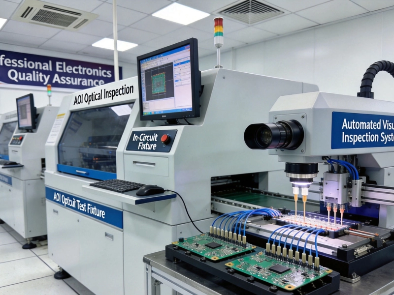
Test type: Flying probe performs electrical testing. Aoi performs visual inspection of solder joints and components.
Defect detection: Flying probe detects electrical opens, shorts, and component value issues. Aoi detects solder defects, missing components, and placement errors.
Complementarity: The methods are complementary, not competitive. Many manufacturers use both AOI and flying probe testing for comprehensive quality control.
Scope: Flying probe tests structural aspects (continuity, components). Functional Testing verifies operational performance.
Power application: Some flying probe systems can apply limited power, but functional testing typically applies full operational power.
Test coverage: Flying probe provides comprehensive structural coverage. Functional testing verifies end-to-end functionality but may miss some structural issues.
Typical use: Flying probe for manufacturing defect detection. Functional testing for performance verification.
Optimizing PCB designs for flying probe testing improves test coverage and effectiveness:
Include dedicated test points at strategic locations throughout the design. Test points should be accessible to probes, ideally on a regular grid to minimize probe travel time. Provide test points for all nets, particularly those that are otherwise difficult to access. Test points should be large enough for reliable probe contact (minimum 0.8mm diameter recommended).
Maintain adequate spacing between test points and other features to accommodate probe bodies and prevent accidental shorts. A minimum spacing of 1.5mm between test points and 2.5mm between test points and component edges provides adequate clearance for most probe systems. Consult your test equipment specifications for exact spacing requirements.
Place test points on the same side of the board where possible to minimize probe flipping and reduce test time. When test points must be on both sides, group them logically to minimize probe repositioning. Avoid placing test points under components or in areas where probe access is restricted.
Ensure every electrical net has at least one accessible test point. For Differential Pairs, provide test points on both conductors. For power and ground nets, provide multiple test points distributed across the board to verify proper connectivity and detect partial opens.
Design circuits to allow in-circuit component testing where possible. This includes providing test access to component terminals and avoiding circuits that prevent component isolation during testing. Some components may require special test considerations or may not be testable in-circuit with flying probe methods.
For panelized PCBs, include test points on each individual board and provide fiducial marks for accurate alignment. Ensure Panel Design doesn't interfere with probe access to individual board test points. Consider whether testing should occur before or after depaneling based on your process flow.
Implement these best practices to maximize flying probe testing effectiveness:
Develop test programs that provide comprehensive coverage while optimizing test time. Include continuity tests for all nets, resistance measurements for critical traces, component testing where applicable, and any special tests required for your specific application. Use automated test program generation tools but review and optimize programs manually for efficiency and completeness.
Implement a regular probe maintenance schedule based on usage and manufacturer recommendations. Replace probe tips before they wear to the point of affecting contact reliability. Clean probes regularly to remove contamination that could affect measurements. Document maintenance activities and track probe life to optimize replacement intervals.
Calibrate measurement instruments regularly according to manufacturer specifications and quality system requirements. Use traceable calibration standards and maintain calibration records. Perform daily verification tests using known standards to confirm measurement accuracy before production testing.
Implement strict version control for test programs, especially when supporting multiple board revisions or product variants. Maintain clear documentation linking test program versions to specific board designs and revision levels. This prevents using incorrect test programs that could produce false results or miss actual defects.
Analyze test results not just for pass/fail decisions but for trends that indicate process shifts. Monitor measurement values over time to detect gradual changes that might indicate developing problems. Use statistical process control techniques to identify when processes are drifting toward specification limits.
Ensure operators are thoroughly trained on flying probe testing equipment, procedures, and troubleshooting. Well-trained operators can identify equipment issues, interpret test results correctly, and respond appropriately to problems. Regular refresher training keeps skills current and introduces new techniques or capabilities.
Integrate flying probe testing into your overall Quality Management System. Establish clear acceptance criteria, define corrective action processes for failures, and maintain traceability of test results to specific production units. Use test data for Continuous Improvement of both design and manufacturing processes.
Flying probe technology continues evolving with new capabilities and applications:
Newer flying probe systems incorporate faster motion systems, improved probe designs, and optimized test algorithms that significantly reduce test times. Some high-speed systems can approach test times comparable to bed-of-nails testing for moderate-complexity boards, making flying probe testing viable for higher volume applications than previously possible.
Advanced flying probe systems incorporate improved measurement capabilities that enable more comprehensive component testing. This includes better capacitance and inductance measurement, semiconductor device testing, and even some functional testing capabilities. These expanded capabilities reduce the need for separate testing stages.
Artificial intelligence and machine learning are being applied to test program generation, automatically optimizing test sequences for speed while maintaining coverage. These systems can learn from previous test programs and human expertise to continuously improve test efficiency.
Modern flying probe systems integrate more seamlessly with manufacturing execution systems (MES), providing real-time quality data to production management systems. This integration enables faster response to quality issues and better overall process control.
Advances in probe design enable testing of smaller test points and finer pitch components. Miniaturized probes maintain contact reliability while accessing test points that were previously too small or closely spaced for flying probe testing.
Consider these factors when selecting a flying probe testing system for your operations:
Determine your required test throughput based on production volume and available test time. Calculate the number of boards you need to test per day or per shift, and ensure the system can meet this requirement including setup time and any retesting needs.
Ensure the system can accommodate your maximum board size and complexity. Consider the number of test points required, component density, and any special testing needs. Verify that probe travel range, Z-axis travel, and other physical specifications match your requirements.
Evaluate the measurement instruments and capabilities against your testing needs. Consider required measurement accuracy, resistance range, capacitance and inductance measurement capabilities, and any specialized measurement requirements your applications may have.
Assess the software capabilities for test program generation, result analysis, and integration with your systems. Look for features like automated program generation, statistical analysis, report generation, and data export capabilities that match your quality system requirements.
Consider the manufacturer's support capabilities, training offerings, and service response times. Reliable support and quick service response minimize downtime and ensure you get maximum value from your investment.
Look beyond initial purchase price to consider total cost of ownership including maintenance, probe replacement costs, software updates, training, and expected lifespan. Consider how the system's capabilities will match your future needs as your products and volumes evolve.
Flying probe testing has established itself as an essential tool in industrial Pcb Quality Control, offering unparalleled flexibility for prototype testing, low-volume production, and High-mix Manufacturing environments. The elimination of custom fixtures, rapid programming, and excellent measurement accuracy make flying probe testing the ideal choice for many applications where traditional bed-of-nails testing proves impractical or uneconomical.
As PCB technology continues advancing with higher component densities, smaller feature sizes, and increased complexity, flying probe testing evolves alongside, incorporating faster systems, enhanced measurement capabilities, and smarter software. The technology's fundamental advantages—flexibility, speed of setup, and cost-effectiveness for appropriate volumes—ensure its continued importance in comprehensive PCB quality control strategies.
Successful implementation of flying probe testing requires understanding its capabilities and limitations, designing boards for testability, implementing best practices, and selecting equipment that matches your specific needs. When applied thoughtfully as part of an overall quality strategy, flying probe testing helps ensure reliable PCBs while maintaining the agility and cost-effectiveness that modern manufacturing demands.
Flying probe testing is significantly slower than bed-of-nails testing. While bed-of-nails testers can test complex boards in seconds, flying probe testing typically takes several minutes to over an hour per board depending on complexity and test coverage. This speed difference makes flying probe testing better suited for low to medium volumes, while bed-of-nails testing excels at high-volume production.
No, flying probe testing doesn't replace all other testing methods but rather complements them. It provides excellent structural electrical testing but doesn't replace visual inspection (AOI) for solder joint quality or functional testing for operational verification. The most comprehensive quality control strategies use multiple testing methods in combination.
Flying probe testing systems range from approximately $30,000 for basic models to $200,000+ for high-end systems with advanced capabilities. Mid-range systems suitable for most industrial applications typically cost $75,000-$125,000. This represents a significant investment but is considerably less than comparable bed-of-nails systems, and there are no ongoing fixture costs.
Probe replacement intervals vary based on usage, board characteristics, and contact force. Typical replacement intervals range from 50,000 to 200,000 contacts per probe tip, but this can vary significantly. Implement a monitoring program to track contact count and measurement quality, replacing probes proactively before they cause test issues.
Flying probe testing can test many component types in-circuit, including resistors, capacitors, inductors, and some semiconductors. However, not all components are testable in-circuit—some require specific test conditions, isolation from surrounding circuits, or functional testing that flying probe systems cannot provide. Component testability should be considered during design.
Identifying and Fixing Micro-Vias Issues in Industrial PCB Quality InspectionsSeptember/10/2026
How to Implement a Robust Quality Assurance Plan for Industrial PCBsJuly/07/2026
Environmental Stress Screening (ESS) for Validating Industrial PCB QualityAugust/08/2026
Why Electrical Testing is Non-Negotiable for Industrial PCB QualitySeptember/29/2026
The Impact of Surface Roughness on High-Speed Signal IntegrityOctober/13/2026
Understanding IPC Class 3 Standards for High-Reliability Industrial PCBsJune/11/2026
Essential Quality Control Tests for Industrial PCBs- ICT, FCT, and AOIMay/27/2026
Minimizing Signal Loss and Crosstalk in High-Speed PCB LayoutsSeptember/01/2026