Open Nav


Power electronics push Pcb Design into territory that standard digital design practices rarely encounter. Where a digital signal trace carries milliamps and dissipates milliwatts, a power bus bar trace must conduct tens or hundreds of amps while managing thermal loads that would destroy ordinary copper. The design rules that govern these high-current interconnects—trace width, copper weight, temperature rise, and manufacturing constraints—form a specialized discipline that stands apart from the signal integrity concerns that dominate most Pcb Design discussions.
Designing heavy copper traces incorrectly doesn't just produce marginally poor performance—it produces failures. Overloaded power traces generate heat that delaminates substrates, destroys solder joints, and ultimately burns open like a fuse. The design rules exist because the physics of high-current conduction demand specific solutions, and violating those rules reliably produces predictable failures. This article explains the engineering principles behind heavy copper trace design, provides practical guidelines for implementation, and addresses the manufacturing considerations that determine whether your design can actually be built.
Understanding heavy copper design starts with the physics of electrical conduction. Current flowing through a conductor produces heat proportional to the power dissipated, which equals I²R—the square of current multiplied by resistance. This relationship is unforgiving: doubling the current quadruples the power dissipation. A trace carrying 10 amps at a given resistance dissipates 100 times the heat of a trace carrying 1 amp at the same resistance.
Resistance itself depends on the conductor's cross-sectional area and material properties. Longer traces have higher total resistance than shorter traces carrying the same current, meaning the same trace width produces different temperature rises at different lengths. Temperature affects resistance further—copper's resistivity increases approximately 0.4% per degree Celsius—creating a thermal feedback loop where heating increases resistance, which increases heating. Understanding these interdependencies explains why simplified design tables, while useful, cannot capture the full complexity of real power trace behavior.
The skin effect becomes significant at high frequencies, pushing current toward the conductor surface and effectively reducing the cross-sectional area available for conduction. For power electronics operating at line frequencies (50-60 Hz) or low-frequency PWM switching, skin depth remains substantial—approximately 8.5mm at 60 Hz in copper—so the effect is negligible for practical PCB trace dimensions. At higher switching frequencies above 100 kHz, skin effect begins reducing effective conductor area, though this is typically less critical than the DC resistance considerations that dominate most power electronics designs.
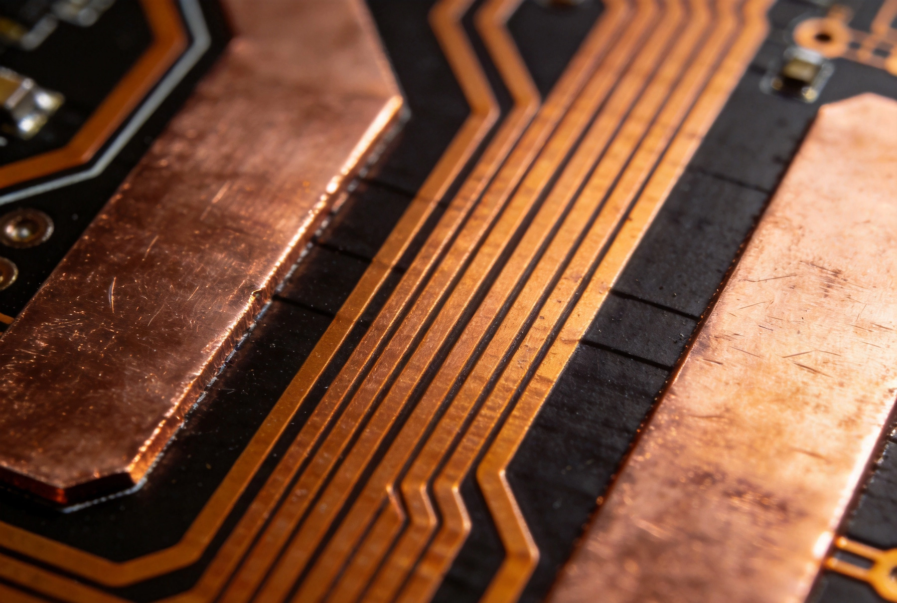
Copper weight—the mass of copper per square foot of board area—is the fundamental parameter that determines a trace's current-carrying capacity. Standard PCB construction uses 1 oz copper per square foot (approximately 35 microns or 1.4 mils thickness) as a baseline. Heavy copper designs typically start at 2 oz and extend to 10 oz or more for extreme power applications.
The relationship between copper weight and current capacity isn't linear. Doubling copper weight more than doubles current capacity because the thermal path from the conductor to the surrounding substrate improves with thickness. Thicker copper also provides more cross-sectional area for heat spreading along the trace length, reducing localized hot spots. This benefit has practical limits—the substrate's thermal conductivity becomes the bottleneck for heat removal from the conductor surface, so beyond a certain copper thickness, additional copper provides diminishing returns.
Standard PCB fabrication processes accommodate copper weights up to approximately 3 oz routinely, with thicker weights requiring specialized processing. The plating process used to build up copper thickness—typically acid copper electroplating—can produce heavier weights, but the process parameters must be controlled carefully to achieve uniform thickness across the panel. Inconsistent copper distribution produces traces with varying current capacity, creating reliability risks that only manifest in field failures.
Each copper weight range suits specific application requirements. Matching copper weight to current requirements—rather than over-specifying unnecessarily heavy copper—optimizes cost and manufacturability without sacrificing performance.
Designing trace width for specific current and temperature rise requires reliable data. The IPC-2152 standard, revised in 2009, provides the most widely accepted baseline for PCB current-carrying capacity, replacing the older and less accurate IPC-2221 charts that preceded it. Understanding IPC-2152's methodology—and its limitations—enables more accurate trace design than rule-of-thumb methods.
IPC-2152 derives current capacity from thermal considerations rather than fusing current. The standard defines charts and equations that relate current, cross-sectional area, temperature rise, and trace length to determine whether a given geometry stays within acceptable temperature limits. The charts account for the thermal environment—the board's position relative to forced air, still air, or external heat sinks—as well as the board's layer structure, copper weights, and proximity to power planes.
A critical insight from IPC-2152 is that external traces carry current more effectively than internal traces. Surface traces dissipate heat to the surrounding air more efficiently than traces sandwiched between substrate layers, which can only shed heat through the surrounding laminate. An external trace carrying 30 A at 20°C rise might require 200 mils width, while the same current in an internal layer might require nearly double that width for identical temperature rise. Design for the actual layer assignment of each trace.
The standard also reveals that trace width matters less than cross-sectional area for current capacity. A trace that is twice as wide but half as thick carries the same current at the same temperature rise. This equivalence matters for manufacturing: a very wide, moderately thick trace might be replaceable with a narrower but heavier copper trace that fits better within routing constraints.
For practical design work, engineers combine IPC-2152 data with calculation tools and engineering judgment. The basic approach:
First, determine the maximum current your trace must carry, including any transient or pulse loads that might exceed continuous current ratings. Second, establish the acceptable temperature rise above ambient—typically 10-20°C for reliable long-term operation in benign environments, up to 40°C or higher for short pulses or harsh thermal environments. Third, select the copper weight appropriate for your current level and manufacturing constraints. Fourth, calculate or look up the required trace width for your combination of current, temperature rise, and layer assignment.
These calculations are necessarily approximate because the actual thermal environment varies with component placement, airflow patterns, nearby heat sources, and the board's mounting configuration. Engineers experienced with power designs typically add 20-30% margin to calculated requirements, accepting some efficiency penalty in exchange for robustness against thermal uncertainties.
Trace width calculations establish a starting point, but Thermal Management strategies amplify trace capacity beyond what copper geometry alone can achieve. The most effective power trace designs incorporate multiple thermal enhancement strategies that work together to keep temperatures within acceptable limits.
Thermal relief patterns connect power traces to pads, allowing solder to flow freely without flooding the entire trace with molten metal during assembly. While essential for manufacturing, thermal reliefs also reduce effective thermal mass at the connection point—heat must flow through the narrow relief spokes rather than directly into the pad. For high-current traces, full thermal relief (solid pad connections) provides better thermal performance but requires careful assembly planning to avoid solder flow problems.
Solder Mask affects thermal performance in subtle ways. An unmasked external trace dissipates heat more effectively to the surrounding air but is also more susceptible to oxidation and handling damage. Masked traces maintain cleaner surfaces but sacrifice some thermal performance. For extreme power applications, removing mask from heavy copper bus bars—exposing bare copper for direct thermal contact with heatsinks or bus bars—provides additional thermal paths that dramatically improve heat spreading.
Thermal Vias placed along high-current traces provide vertical heat paths to inner ground and power planes. The copper plating inside Thermal Vias conducts heat efficiently into the plane layers, which act as thermal spreading planes that distribute heat across the board. This technique works particularly well when the trace runs between plane layers that provide thermal mass and spreading area. A trace flanked by ground planes can carry significantly more current than the same trace on a surface layer with no adjacent planes.
The most carefully calculated trace design is worthless if it cannot be manufactured reliably. Heavy Copper Pcb fabrication introduces process challenges that standard designs avoid, and designing without these constraints in mind produces boards that either cannot be built or cost far more than anticipated.
Chemical etching—the process that removes unwanted copper to leave traces—undercuts traces from the side, producing traces that are wider at the base than at the top. This effect is proportional to etch depth: the deeper the etch removes copper, the wider the undercut. Standard 1 oz copper on typical board thicknesses produces negligible undercut, but heavy copper traces etched through thick copper produce noticeably tapered cross-sections that deviate significantly from the intended geometry.
Designers must compensate for etch factor by specifying traces narrower than the final desired width, accounting for the expected undercut during etching. The required compensation depends on copper weight, board thickness, and the specific etch chemistry used—information that varies between fabricators. Communicating with your manufacturer about their etch factor and adjusting designs accordingly prevents the frustrating discovery that fabricated traces don't match calculations.
Alternative fabrication approaches mitigate etch factor challenges. Additive plating processes, which build up copper rather than removing it, produce traces with vertical sidewalls and precise dimensional control. These processes cost more than subtractive etching but eliminate the undercut problem entirely. For extreme power applications where dimensional precision is critical, the additional cost may be justified by performance benefits.
Heavy copper boards built with electroplated copper often exhibit non-uniform thickness across the panel. Current density concentrates at edges and corners during plating, producing thicker copper in these areas than in the panel center. This non-uniformity affects trace current capacity—traces at the panel edge might carry significantly more current than traces in the center, creating subtle reliability risks that don't appear in testing.
Quality fabricators address plating uniformity through panel design (thieving patterns that equalize current distribution), process control (careful bath chemistry management), and sometimes selective plating that targets heavy copper areas specifically. Discussing plating uniformity requirements with your manufacturer, and requesting thickness distribution data for critical builds, helps you understand and manage this variability.
High-current paths rarely stay entirely on the surface plane. Vias carry current vertically through the board stackup, and their current capacity becomes critical for power distribution networks. A single 10-mil plated through-hole cannot carry 30 A regardless of how wide the adjacent trace is—the current must crowd through the small plating cross-section, generating localized heat that damages the barrel.
Multiple smaller vias, staggered to distribute current, often carry more total current than fewer larger vias because the current distributes more uniformly across the available plating. For very high current, copper-filled or copper-overfilled vias provide current capacity approaching that of solid copper bars. These specialized via structures cost significantly more than standard through-holes but enable current densities that would otherwise require bus bars or external wiring.
Translating the principles above into actionable design rules requires practical guidelines that account for real-world manufacturing and assembly constraints.
Maintain minimum trace spacing appropriate to the voltage between adjacent conductors. High-current traces often carry voltage potentials that differ significantly from neighboring circuits, and creepage and clearance requirements must accommodate the maximum voltage difference. For low-voltage power distribution, spacing is less critical; for high-voltage designs, spacing requirements can dominate the layout area consumed by power traces.
Use rounded trace corners rather than sharp 90-degree angles. While the electrical impact of corner geometry is negligible at DC and low frequencies, sharp corners concentrate etchant during manufacturing and can create stress concentrations that crack traces under Thermal Cycling. A 45-degree miter or generous radius improves manufacturing yield and reliability without any electrical penalty.
Connect heavy copper traces to component pads with appropriately sized thermal reliefs or full-contact pads. Small component pads cannot accept the full current that a heavy bus bar carries—current must enter or exit through the component leads or termination. Designing terminations that match the current path to component capabilities prevents localized heating at the connection point.
When designing heavy copper boards, early engagement with the fabricator prevents expensive surprises. Not all PCB shops can reliably produce boards with copper weights above 3 oz, and those that can may have specific design restrictions—a minimum trace width for heavy copper, a maximum heavy copper area per panel, or panel size limitations for heavy plating processes. Sharing your design files for a preliminary manufacturability review identifies these constraints before tooling commits.
Panel utilization considerations affect heavy copper boards differently than standard boards. Heavy copper plating costs are often quoted by the panel area processed, not by the amount of copper deposited—so a design that uses 90% of the panel surface pays nearly the same plating cost as one using 50%. This pricing structure can make heavy copper economically unattractive for low-density designs that waste panel area.
Walking through a practical design example illustrates how these principles combine in real applications. A 50A brushless DC motor drive requires a power bus carrying the full motor current from the DC link capacitors to the inverter MOSFETs—a distance of approximately 50mm across the board.
Using IPC-2152 with 2 oz copper, 20°C temperature rise, external layer, and 50mm trace length, the required trace width calculates to approximately 600 mils (15mm)—impractically wide for a compact layout. Adding thermal vias connecting to adjacent ground planes distributes heat into the plane layers, reducing the required surface trace width to approximately 300 mils while maintaining the same temperature rise. Using 3 oz copper further reduces width to approximately 200 mils, a manageable dimension for a medium-sized board.
The final design uses 3 oz copper on both outer layers, with thermal vias on 5mm pitch connecting to solid power and ground planes in the inner layers. This structure distributes current across all available copper, spreading the thermal load and providing redundant current paths that maintain function even if a single via fails. Total power bus width of approximately 200 mils fits within the layout while providing comfortable margin against the 50A requirement.
Several recurring Design Errors consistently cause problems in power electronics PCBs. Avoiding these mistakes saves debugging time and prevents field failures.
Assuming trace width alone determines current capacity ignores the thermal environment. A trace calculated for 30°C rise in still air will far exceed 30°C rise if the board operates in an enclosure with limited airflow, near heat-generating components, or at elevated ambient temperatures. Designing for the actual thermal environment—not an optimistic ideal—prevents thermal runaway in the field.
Using insufficient vias to connect power traces between layers creates current density hot spots at the barrel plating. The common shortcut of using a single via to transition a power trace between layers creates exactly this problem. Designing arrays of vias with adequate current-sharing ensures reliable current transfer without localized overheating.
Neglecting the thermal resistance of the solder joint that terminates the power trace often becomes the weakest link. A trace calculated for 50A that terminates in a component lead rated for 30A fails because the weakest link—the solder joint—determines system performance. Reviewing termination current ratings and designing connections that match trace current capacity ensures the system performs as the trace calculations suggest.
Using IPC-2152 for an external trace in still air with 20°C temperature rise, a 100 mil (2.5mm) wide, 2 oz copper trace carries approximately 8-10 A depending on trace length and specific thermal conditions. Longer traces run hotter for the same current due to cumulative heating. Internal traces carry less current—approximately 6-8 A for the same geometry—due to reduced Heat Dissipation to adjacent planes. These numbers serve as starting estimates; actual performance depends on your specific thermal environment.
For most power electronics designs, copper pour provides superior thermal performance because it spreads current across a large area, reducing current density and improving heat spreading. Dedicated traces with precise widths waste the thermal spreading benefit of large copper areas. Use polygon pours for power distribution wherever routing constraints allow, and reserve precise trace widths for situations where copper pour would create unintended connections or manufacturing complications.
Standard surface finishes—HASL, ENIG, OSP—work with heavy copper boards without special modifications. The finish is applied to the surface copper, not the bulk copper thickness, so finish selection is independent of copper weight. However, heavy copper boards with heavy plating may exhibit slightly different finish appearance (thicker ENIG may look different than standard thickness) without affecting functional performance.
Yes, and mixing copper weights is a common technique for optimizing cost and performance. Heavy copper for power distribution on outer layers combines with standard copper for signal traces, reducing the total cost of the panel plating process. Mixed-copper designs require careful design documentation to specify which areas receive heavy copper, and fabricators may charge a premium for the additional processing steps. Discuss mixed-weight designs with your manufacturer early to confirm process capability and pricing.
PCB fabricators commonly quote 3-6 oz as their standard heavy copper range, with specialty shops capable of 10 oz or more. Above 6 oz, manufacturing costs increase substantially, plating uniformity becomes more difficult to control, and drilling characteristics change. For applications requiring more than 6 oz copper, alternative approaches—metal-core PCBs, copper bus bars soldered to the board, or hybrid assemblies—often provide better cost-effectiveness than attempting extreme copper weights in standard board construction.
Heavy copper trace design for power electronics combines Thermal Management, materials science, and manufacturing knowledge in ways that standard PCB design practice doesn't prepare most engineers for. The fundamental relationship between current, temperature rise, and cross-sectional area provides the starting point, but the details—layer assignment effects, thermal relief design, etch factor compensation, via current capacity, and manufacturing constraints—determine whether a design succeeds or fails in practice.
The most reliable approach combines careful calculation using IPC-2152 or equivalent data with appropriate engineering margin, thermal enhancement strategies that amplify copper capacity beyond geometry alone, and early collaboration with your fabricator to confirm manufacturing feasibility. Designing heavy copper without these inputs produces boards that may work in limited testing but fail in the thermal and electrical stress of real-world operation.
Power electronics PCB design rewards the attention to detail that heavy copper demands. The investment in understanding these design rules—and implementing them carefully—produces boards that perform reliably through years of service, rather than failing prematurely under the thermal stress that power electronics inevitably impose.
Designing power electronics with demanding current requirements? Our engineering team specializes in high-current PCB design and heavy copper manufacturing. Share your design files for a DFM review that addresses thermal and manufacturing challenges before production.
How to Avoid Costly Mistakes with Proper Industrial PCB DFMJuly/03/2026
Essential Rules for Industrial PCB DesignJune/08/2026
Design for Testability (DFT): A Crucial Aspect of Industrial PCB DesignJuly/20/2026
Essential Rules for Industrial PCB DesignMay/27/2026
A Comprehensive Guide to High-Tg Materials for Industrial PCBsMay/27/2026
Key Differences Between Consumer and Industrial PCB ProductionJune/27/2026
Navigating the Complexities of Box Build AssemblyMay/27/2026

SMT vs. Through-Hole: Best Practices for Industrial PCBAJuly/07/2026