Open Nav


Industrial PCB Fabrication produces the foundation for reliable electronic assemblies, but the manufacturing process introduces numerous opportunities for defects that compromise quality. Understanding common defects, their root causes, and effective prevention strategies enables manufacturers to achieve higher yields and more reliable products. When defects do occur, systematic analysis and corrective action prevent recurrence and improve process capability. This article explores the most prevalent PCB Fabrication defects and provides practical guidance for overcoming them in industrial production environments.

Fabrication defects create cascading costs that extend far beyond scrap material. When defective boards reach assembly lines, they cause production delays while manufacturing engineers investigate root causes. Assembly yields drop because defective boards cannot be completed. Field failures emerge when latent defects survive to final products, creating warranty costs and customer dissatisfaction. These impacts compound when defects reach high-volume production, where a single defect mechanism can affect thousands of units before detection.
The financial impact includes obvious costs like material scrap and rework, but also hidden costs like engineering investigation time, production line downtime, and customer service response. Defect analysis and corrective action consume valuable engineering resources that could drive new product development. Understanding these costs justifies investment in defect prevention and early detection systems that reduce total cost of quality over time.
Delamination occurs when copper layers or dielectric material separate within the multilayer stackup. This defect typically manifests as air pockets or separation visible through transparent materials or through X-ray inspection. Delamination creates catastrophic failures because it breaks electrical connections and introduces mechanical weakness. Common causes include inadequate lamination pressure, insufficient cure time, moisture contamination in materials, and thermal expansion mismatch between materials during subsequent thermal processing.
Moisture absorption represents a particularly insidious cause of delamination. FR4 and other dielectric materials absorb atmospheric moisture, which vaporizes explosively during lamination when moisture content exceeds allowable limits. Boards with absorbed moisture often show blistering or delamination after high-temperature exposure during soldering operations. This delayed manifestation makes moisture-related delamination especially problematic because boards may pass initial inspection but fail later during assembly or field use.
Preventing delamination starts with material handling and storage. Store dielectric materials in controlled humidity environments with moisture barrier packaging. Perform bake-out procedures on materials with unknown moisture history before lamination. Implement strict material receiving inspections that verify moisture content using weight gain measurements or specialized moisture analyzers.
Process parameters for lamination require careful control and monitoring. Maintain appropriate lamination pressure throughout the entire cycle, ensuring uniform pressure distribution across the panel surface. Verify that lamination temperature profiles match material specifications, with adequate soak times to ensure complete polymerization. Implement in-process monitoring that detects pressure or temperature excursions that could compromise lamination integrity.
Copper shorts occur when conductive paths exist where they should not, creating unintended electrical connections. Shorts manifest as shorts between traces, shorts between layers, or shorts to ground or power planes. Common causes include over-etching that bridges adjacent traces, copper debris that contaminates surfaces, insufficient etch resist coating, and plating defects that create unintended copper deposits.
Copper debris represents a pervasive cause of shorts that occurs throughout the fabrication process. Drilling operations generate copper burrs that can create bridges if not completely removed. Mechanical abrasion during handling creates fine copper particles that settle on surfaces and embed in resist layers. These latent shorts may not manifest until electrical testing or assembly operations when Thermal Cycling causes debris to move and create electrical contact.
Open circuits occur when intended conductive paths are incomplete or interrupted. Truncated traces, incomplete plating, and damaged copper create high-resistance or infinite-resistance connections that prevent proper electrical operation. Open circuits often result from under-etching that leaves traces too narrow, mechanical damage during handling, or plating failures that leave through-holes or vias with insufficient copper coverage.
Over-etching represents the most common cause of open circuits in trace patterns. When etch parameters favor copper removal too aggressively, trace dimensions shrink below design minimums and eventually break completely. The problem compounds with fine-pitch designs where trace widths approach fabrication capability limits. Tightening process controls and implementing design rules that account for etch bias reduces over-etching risks.
Preventing shorts and opens requires comprehensive process control combined with robust electrical testing. Implement automated optical inspection (Aoi) after each major process step to detect visual defects before they propagate through subsequent processing. Use electrical testing, including continuity and isolation testing, to verify electrical integrity before boards advance to assembly.
Design For Manufacturability practices significantly reduce short and open risks. Maintain adequate trace spacing based on fabrication capability limits. Avoid trace widths that approach the minimum capability of the fabrication process. Provide sufficient annular rings around plated holes to ensure complete plating coverage even with minor alignment variations.
Plating voids occur when plated through-holes or surface finishes contain gaps or insufficient metal coverage. Voids in plated through-holes create high-resistance connections that can fail under current load or Thermal Cycling. Surface finish voids expose underlying copper, creating reliability risks from oxidation and poor solderability. Common causes include poor surface preparation, contamination in plating baths, and inadequate plating time.
Plating voids in through-holes represent particularly challenging defects because they occur inside structures that are not visible from board surfaces. These voids can remain undetected unless X-ray inspection or electrical testing specifically targets them. When voids create partial connections, resistance may appear acceptable during low-current testing but fail under operating conditions where current flow generates heat that exacerbates the defect.
While insufficient plating creates problems, excessive plating causes different manufacturing issues. Over-plated through-holes may not fit component leads, causing assembly difficulties. Over-plated surface features can interfere with solder paste printing and component placement. Plating beyond specified thickness also creates cost overruns and unnecessary material consumption.
Over-plating typically results from excessive plating time or overly aggressive plating current density. Process monitoring that tracks plating rate and automatically terminates plating when target thickness is achieved prevents over-plating. However, thickness variations across large panels create challenges when some areas reach target thickness while others require additional plating.
Implement statistical process control (SPC) for plating operations to detect process drift before it creates defects. Monitor plating rate, bath chemistry, and current density continuously. Establish control limits that alert operators to conditions requiring intervention before defective material is produced.
Cross-section analysis provides the most direct verification of plating quality. Implement sampling plans that require periodic cross-sectioning of production panels, focusing on critical features like through-holes, Blind Vias, and surface plating. X-ray inspection offers non-destructive alternatives for detecting plating voids, particularly for high-value applications where destructive testing is impractical.
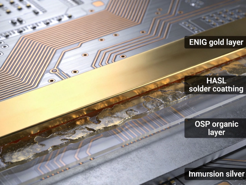
Surface finishes protect copper from oxidation and provide solderable surfaces for component attachment. When finishes degrade through oxidation, contamination, or mechanical damage, solderability suffers and assembly yields drop. Common surface finish problems include oxidized copper exposed through thin finish layers, contamination from handling or processing chemicals, and scratches that expose underlying copper.
Electroless nickel immersion gold (ENIG) finishes present specific failure modes. Hyper-corrosion creates black spots on nickel surfaces that prevent solder wetting. Immersion gold layer thickness that is too thin exposes nickel to corrosion. Gold embrittlement occurs when excessive gold dissolves into solder during assembly, creating brittle joints. Each of these mechanisms requires specific process controls to prevent.
Solder Mask defects create both cosmetic and functional problems. Misregistered Solder Mask exposes copper where protection is needed, leading to shorts during assembly. Solder mask bridging between pads prevents proper solder paste deposition and component placement. Mask adhesion failures cause mask delamination during thermal cycling, exposing copper and creating reliability risks.
Solder mask application requires precise control of exposure and development parameters. Insufficient exposure leaves resist that should be removed, creating bridging. Over-exposure weakens adhesion and can cause mask lifting. Development time and temperature must balance complete removal of unexposed resist against preservation of exposed mask features.
Registration errors occur when layer-to-layer alignment drifts beyond specified tolerances. Misalignment causes features like through-holes to miss their intended connection points, creating opens or incomplete connections. Registration errors compound across multiple layers, with small alignment variations accumulating to create significant dimensional errors in complex multilayer boards.
Registration control requires precise alignment systems and monitoring throughout the fabrication process. Implement vision systems that verify alignment before each imaging step. Track registration across process stages to identify drift before it exceeds acceptable limits. Use reference features like fiducial marks to establish coordinate systems that enable layer-to-layer alignment verification.
Warping occurs when boards become non-planar, creating difficulty during assembly and potential reliability problems. Uneven copper distribution, asymmetric stackup constructions, and thermal stress from processing all contribute to warping. Warped boards do not sit flat during assembly, causing pick-and-place errors and solder paste thickness variations.
Preventing warping requires balanced copper distribution across layers and symmetric stackup constructions. When designs require asymmetric copper distribution, implement stress-relief patterns that balance the copper masses. Control thermal ramp rates during processing to minimize thermal stress buildup. Implement handling procedures that prevent mechanical stress that can induce warping.
Effective defect analysis requires systematic root cause investigation. When defects occur, implement a structured approach that gathers data, identifies potential causes, tests hypotheses, and implements corrective actions. Tools like fishbone diagrams, 5-why analysis, and fault tree analysis provide frameworks for systematic investigation.
Data collection is critical to effective root cause analysis. Document defect characteristics including frequency, location, and severity. Identify whether defects correlate with specific process steps, material lots, or equipment. Statistical analysis of defect patterns often reveals root causes that are not obvious from examining individual defective boards.
Implement corrective actions that address root causes rather than symptoms. When a process parameter drifts beyond control limits, recalibrate equipment and implement monitoring that prevents recurrence. When material contamination causes defects, identify contamination sources and implement control measures. The corrective action must directly address the identified root cause to prevent recurrence.
Verification confirms that corrective actions are effective before they are fully implemented into production. Perform pilot runs with enhanced monitoring to confirm that defect rates decrease as expected. Collect data that demonstrates improvement and validates the effectiveness of the corrective action. Only after verification should the change be adopted as standard practice.
What is the most common Pcb Fabrication defect?
While defect types vary by manufacturer and product complexity, electrical shorts and opens generally represent the most common fabrication defects. These defects result from numerous potential causes including etching issues, contamination, and plating problems, making them pervasive across different fabrication environments. Shorts and opens also create immediate functional failures that are readily detected during electrical testing.
How can I reduce fabrication defects in my products?
The most effective approach combines Design For Manufacturability with partner selection and quality monitoring. Design products that respect fabrication capability limits rather than pushing boundaries unnecessarily. Select fabrication partners with demonstrated process capability and quality systems. Implement incoming inspection and monitoring that catches defects early before they propagate through assembly and into fielded products.
What role does moisture play in Pcb Fabrication defects?
Moisture represents one of the most significant causes of latent defects. Absorbed moisture in dielectric materials vaporizes during high-temperature processing, causing delamination, blistering, and other defects. Moisture also promotes corrosion and reduces plating adhesion. Implementing strict moisture control throughout material handling, storage, and processing significantly reduces defect rates.
When should I reject an entire panel versus accepting good boards?
The decision depends on defect type, defect distribution, and application criticality. When defects cluster in specific areas rather than distributing randomly across the panel, rework of affected boards may be feasible. When defects suggest systemic process problems, rejecting the entire panel prevents accepting boards that may have latent defects. For critical applications like military or aerospace, rejection criteria are more stringent than for consumer products.
How do I measure fabrication quality improvement?
Track key metrics including defect rates by defect type, first-pass yield, and customer returns. Establish baseline measurements before implementing improvement initiatives and compare trends over time. Use statistical process control charts to monitor process stability and detect degradation before it creates excessive defects. Financial metrics like cost of quality provide business-level visibility into improvement impact.
Overcoming common PCB fabrication defects requires systematic approaches that combine prevention, detection, analysis, and Continuous Improvement. Understanding defect mechanisms enables designers and manufacturers to implement effective prevention strategies. Robust process controls and quality monitoring catch defects before they create costly impacts. Root cause analysis drives Continuous Improvement that reduces defect rates over time.
The most successful organizations view defect reduction as ongoing improvement rather than one-time initiatives. Establish quality systems that track defects, analyze patterns, and implement corrective actions systematically. Engage fabrication partners as collaborative problem solvers rather than suppliers to be policed. When design and manufacturing teams work together to understand and eliminate defect mechanisms, the entire production ecosystem benefits from improved reliability and reduced cost.
Start by understanding the most common defects in your specific applications and fabrication processes. Implement the highest-impact prevention strategies first, typically addressing moisture control, process parameter management, and design for manufacturability. As defect rates decrease, expand improvement efforts into more complex mechanisms. The cumulative effect of continuous improvement creates significant competitive advantages through higher yields, better reliability, and lower total cost of quality.

How to Choose the Right Manufacturer for Industrial PCB FabricationJune/29/2026
Precision Engineering: Tolerances in High-End Industrial PCB FabricationSeptember/03/2026
Advanced Techniques in Multi-Layer Industrial PCB FabricationJune/03/2026
Predicting Lifespan: Accelerated Life Testing for Industrial PCB ReliabilityAugust/03/2026
The Impact of Surface Finishes on Industrial PCB Fabrication QualityJuly/16/2026
Materials, Methods, and Industry Standards ExplainedMay/27/2026
A Comprehensive Guide to High-Tg Materials for Industrial PCBsMay/27/2026

Innovative Industrial PCB Solutions for Renewable Energy SystemsAugust/11/2026