

Renewable energy is no longer a niche sector. Across the world, solar farms, wind parks, and grid-scale battery storage installations are being deployed at a pace that would have seemed optimistic a decade ago. Behind every megawatt of clean electricity flowing into the grid is a chain of Power Electronics that conditions, converts, and controls the energy — and at the heart of that electronics chain is the printed circuit board. The PCB challenges presented by renewable energy systems are in some respects the most demanding in Industrial Electronics: power levels that challenge conventional Thermal Management, outdoor environments that demand resilience against temperature cycling and humidity, and twenty-year operational life requirements that dwarf the lifecycle of most consumer products. This article examines how PCB designers and manufacturers are meeting those challenges with innovative materials, architectures, and assembly approaches tailored specifically for solar, wind, and energy storage applications.
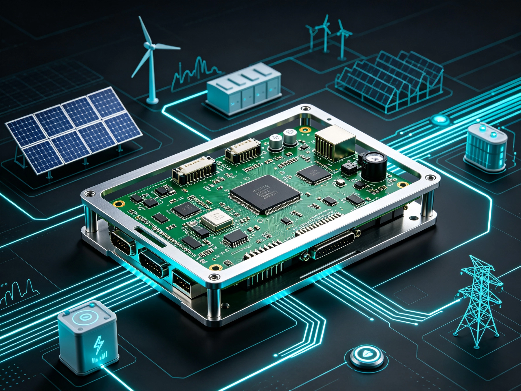
Before diving into specific PCB solutions, it is worth understanding what distinguishes renewable energy electronics from the typical industrial or consumer applications that most Pcb Assembly work serves. The constraints that define the design space for solar inverters, wind turbine converters, and battery management systems are more extreme in several dimensions simultaneously.
First, power levels in renewable energy systems are high relative to most PCB applications. A utility-scale Solar Inverter handling 500 kW to 2 MW of power operates at current and voltage levels that require careful Thermal Management and, in many cases, custom bus bar integration rather than conventional PCB trace routing. Even at the component level, the MOSFETs, IGBTs, and SiC devices used in power conversion generate watts of heat in packages that must interface with the PCB thermal structure reliably.
Second, the operating environment for renewable energy electronics is harsh. Solar inverters are typically mounted outdoors in utility-scale installations, exposed to full sun, rain, dust, and temperatures that swing from below freezing on winter nights to fifty degrees Celsius or more on hot summer afternoons. Wind turbine nacelles are sealed enclosures that experience vibration, temperature extremes, and limited maintenance access. Battery storage systems operate in containerized environments where thermal runaway risk imposes additional constraints. The Pcb Materials, coatings, and connectors in these applications must be specified for the full environmental range, not just the benign interior of a factory floor.
Third, renewable energy systems are expected to operate for twenty to thirty years — the typical payback period for a solar installation or wind farm investment. This lifecycle requirement means that every component on the PCB must have a reliability margin that accounts for degradation over decades rather than years. Capacitors dry out. Solder joints fatigue under Thermal Cycling. Connectors corrode. The engineering discipline required to design for this lifecycle is more demanding than the five to ten year expectations common in most industrial control applications.
Standard Fr-4 Laminate, with a typical Glass Transition Temperature (Tg) of 130 to 140 degrees Celsius, is adequate for many industrial control applications where operating temperatures stay well below that threshold. Renewable energy electronics are different. In a rooftop solar installation, the inverter enclosure can reach sixty degrees Celsius inside on a hot day. In a desert solar farm, ambient temperatures during peak generation hours regularly exceed forty degrees Celsius. The combination of ambient temperature and self-heating from power dissipation means that the PCB inside these enclosures may operate at fifty to eighty degrees Celsius continuously for years on end.
High-Tg and high-Cti laminates address part of this challenge. Laminates with Tg values above 170 degrees Celsius — such as polyimide (PI) and some ceramic-filled hydrocarbon composites — provide a wider margin between operating temperature and the glass transition point. Cti (Comparative Tracking Index) ratings become important in inverter applications where contamination and humidity can create leakage paths across the PCB surface. Laminates with CTI ratings above 400 V provide better protection against tracking failures in damp or polluted environments.
Metal-backed substrates — aluminum IMS (Insulated Metal Substrate) boards and copper-backed substrates — are increasingly used in renewable energy Power Electronics because they combine electrical isolation with high in-plane Thermal Conductivity. An aluminum Ims Board can have a Thermal Conductivity of 1 to 5 W/mK, compared to 0.3 W/mK for standard FR-4. For power modules in Solar Inverter and wind converter applications, IMS substrates allow the thermal path from the semiconductor junction to the metal baseplate to be managed with far less temperature rise than a standard FR-4 stack-up would allow.
At the highest power levels in renewable energy systems — utility-scale solar inverters above 500 kW, full-converters for multi-megawatt wind turbines — discrete PCB-based assembly reaches its practical limits. The current handling required for these power levels is more effectively managed with power modules that use Direct Bonded Copper (DBC) substrates inside the module package. DBC substrates use a ceramic Dielectric Layer (aluminum nitride or alumina) bonded directly to copper on both sides, with the circuit pattern etched into the top copper layer. The ceramic provides electrical isolation at high voltage while offering thermal conductivity an order of magnitude higher than organic dielectrics.
Pcb Assembly for renewable energy systems at these power levels involves mounting the power modules to a thermal bus bar structure, then integrating the module assembly into a larger system PCB that handles signal conditioning, communication, and control. The PCB in this context is less about power handling and more about the intelligence layer — analog front ends for current and voltage sensing, gate driver circuits for the switching devices, microcontroller interfaces, and grid communication protocols. These control PCBs must interface reliably with the high-power modules through connectors and harness assemblies that maintain isolation between the high-voltage and low-voltage domains.
The transition from silicon IGBTs and MOSFETs to silicon carbide (SiC) and gallium nitride (GaN) wide-bandgap semiconductors is happening faster in renewable energy applications than in most other sectors. The higher switching frequencies enabled by SiC and GaN — 50 kHz to 200 kHz versus 2 kHz to 20 kHz for silicon — allow magnetic components in solar inverters and battery converters to shrink significantly, reducing system cost and weight. The higher Breakdown Voltage and superior thermal conductivity of SiC make it particularly well-suited for solar inverter and energy storage applications that operate at 1200 V bus voltage or above.
Pcb Design for SiC and GaN circuits introduces challenges that differ from conventional silicon designs. Higher switching speeds mean that parasitic inductance in the gate drive loop and power loop causes larger voltage overshoots and ringing. Pcb Layout must minimize loop areas with careful attention to gate return paths, decoupling capacitor placement, and power loop commutation areas. The CM's process engineering team must understand these layout requirements during the DFM phase, and the fabricator must be capable of producing boards with tighter registration tolerances and finer trace geometries than a conventional industrial control board.
At these switching frequencies, the PCB dielectric losses become more significant. Low-loss laminates — Rogers RO4000 series, Panasonic Megtron 6, and similar materials with lower dissipation factor than standard FR-4 — are increasingly specified in the power stage sections of SiC-based renewable energy inverters. The additional material cost is justified by reduced dielectric heating at high switching frequencies and improved Signal Integrity for the control circuitry.
Managing PCB temperature in outdoor renewable energy installations is a systems engineering challenge that goes beyond the PCB itself. The thermal path from the semiconductor junction through the PCB, the enclosure, and the external heatsink or cooling system must be optimized as an integrated chain. Each link in that chain — the thermal interface material, the PCB dielectric, the heatsink attachment, the enclosure thermal design, the ambient cooling strategy — contributes to the total Thermal Resistance.
Conformal Coating is commonly applied to PCBs in outdoor renewable energy applications as the first line of defense against humidity and contamination. Acrylic, silicone, and urethane coatings each offer different combinations of Moisture Protection, Thermal Resistance, and reparability. Parylene coating provides superior moisture barrier performance and uniform coverage even on irregular surfaces, but at significantly higher cost and with more limited rework options after coating.
For solar inverter applications where the inverter is mounted directly behind the PV array — increasingly common in residential and commercial installations — the PCB must survive not just high ambient temperatures but Thermal Cycling from daily on-off cycles of the inverter. The Solder Joint Reliability requirements under these conditions are substantial, and boards intended for this application benefit from thermal cycling testing to validate the assembly process before committing to volume production.
Grid-scale battery Energy Storage Systems (BESS) represent the fastest-growing segment of the renewable energy ecosystem, and they impose their own distinct set of PCB requirements. A battery management system (BMS) monitors the voltage, temperature, and state of charge of individual cells in a large battery pack, executing balancing algorithms and protecting against overcharge, overdischarge, and thermal runaway conditions. The PCB requirements for BMS front-end electronics are characterized by high channel count, stringent measurement accuracy, and extremely high reliability demands.
Measurement accuracy in a BMS is critical because the safety of the entire system depends on accurate state-of-charge estimation and cell balancing. The analog front-end ICs that perform cell voltage measurement must be located close to the cell terminals to minimize trace resistance errors, which often means the BMS PCB is physically distributed — one small board per battery module, communicating with a central controller board through an isolated communication bus. The distributed boards must be compact, highly reliable, and specified for the same twenty-year operational life as the rest of the system.
Isolation requirements in BMS PCBs are among the most demanding in electronics. The battery stack in a utility-scale BESS may operate at 1500 V DC or higher, and the BMS electronics that monitor individual cells must maintain isolation between each cell and the overall system bus. Transformers and digital isolators on the BMS PCB must be rated for the full working voltage of the battery stack plus an appropriate safety margin. Creepage and clearance distances on the PCB — the spacing between conductors at different potentials — must be designed to relevant safety standards such as IEC 62109 for solar inverters and UL 9540 for Energy Storage Systems.
Designing a PCB for a twenty-five year operating life requires a Reliability Engineering discipline that goes beyond standard commercial quality levels. The failure modes that matter most over this timescale are Thermal Fatigue of solder joints, degradation of electrolytic and film capacitors, corrosion of metallization and plating, and wear of connectors and contacts. Each of these failure modes can be mitigated through component selection, board design, and assembly process choices, but the mitigation must be intentional — it does not happen automatically.
Thermal cycling testing to accelerated lifecycle standards — typically a temperature range of -40 to +85 or +105 degrees Celsius for outdoor renewable energy applications — is an essential validation step for PCBs in these applications. A board that passes 1,000 thermal cycles without degradation provides confidence that it can survive decades of daily temperature swings in the field. HALT (Highly Accelerated Life Testing) and HASS (Highly Accelerated Stress Screening) protocols are commonly used by leading renewable energy electronics manufacturers to identify design and process weaknesses before production.
Damp heat testing — exposing the board to 85 degrees Celsius and 85 percent relative humidity for 1,000 to 2,000 hours — validates the board's resistance to moisture ingress, which is particularly important for outdoor applications in humid climates. Boards that pass damp heat testing with Conformal Coating are substantially more likely to survive field exposure than boards validated only to standard assembly-level tests.
Sourcing PCB assembly for renewable energy electronics from a contract manufacturer requires careful evaluation of their relevant experience and quality infrastructure. Not every CM that produces excellent consumer or industrial control assemblies has the materials knowledge, process documentation discipline, and testing capability to reliably produce boards for twenty-five year outdoor applications. The questions to ask during CM evaluation are specific: what is their experience with IMS substrates and high-Tg laminates? Can they provide thermal cycling and damp heat test data from comparable assemblies? Do they have a process for tracking and managing long-term material obsolescence, so that a board qualified today can still be reproduced with equivalent materials five years from now?
Turnkey assembly relationships — where the CM manages component sourcing, assembly, conformal coating, test, and delivery as an integrated service — are particularly well-suited for renewable energy electronics. The component counts are manageable, the testing requirements are well-defined, and the long production runs typical of utility-scale deployments reward the investment in process setup that turnkey assembly requires.
Renewable energy systems are pushing PCB technology in directions that conventional Industrial Electronics do not always require. Higher power densities, wider temperature ranges, twenty-five year lifecycle demands, high isolation voltages, and increasingly the adoption of wide-bandgap semiconductor technologies all create design and manufacturing challenges that require intentional engineering rather than default specifications. The most successful renewable energy electronics programs treat the PCB as a system-critical element rather than a commodity, invest in materials and process qualification upfront, and work with contract manufacturing partners who bring relevant experience and Reliability Engineering discipline to the relationship. As the renewable energy sector continues its rapid growth trajectory, the Pcb Supply Chain that serves it will need to raise its capabilities in parallel — and the manufacturers and designers who build that expertise now will be well-positioned for the decades ahead.
Material Selection Guide for High-Speed Industrial PCB SolutionsJuly/14/2026
Tailored Industrial PCB Solutions for Medical Device ManufacturersJune/12/2026
Manufacturing Processes Unique to Rigid-Flex PCB SolutionsOctober/10/2026
Rapid Prototyping Services: Fast-Tracking Your Industrial PCB SolutionsSeptember/30/2026

Cost Analysis: Is Rigid-Flex the Right Solution for Your Industrial Project?September/15/2026
Manufacturing Challenges in 20+ Layer Industrial PCB SolutionsJuly/09/2026
Custom Industrial PCB Solutions for the Automotive SectorMay/27/2026
Rogers vs. PTFE: Comparing Materials for High-Frequency SolutionsSeptember/17/2026