Open Nav


Signal Integrity has become one of the defining challenges in modern Electronics Design, as increasing data rates and shrinking geometries push traditional PCB approaches toward their fundamental limits. High-layer Count boards and high-density interconnect technology represent the industry's primary responses to these challenges, offering capabilities that address Signal Integrity concerns at their root rather than merely treating symptoms. Understanding how these technologies affect signal propagation, crosstalk, and electromagnetic emissions enables designers to make informed architectural decisions that determine product performance.
The transition from traditional Pcb Design to High-layer Count and HDI solutions represents a fundamental shift in approach rather than simply an increase in layer numbers. While additional layers certainly provide routing flexibility, the real benefits emerge from the ability to implement proper reference planes, Controlled Impedance structures, and optimized layer stacking. Hdi Technology extends these capabilities further by enabling microvia structures that minimize discontinuities and support the fine geometries required for modern high-speed interfaces.
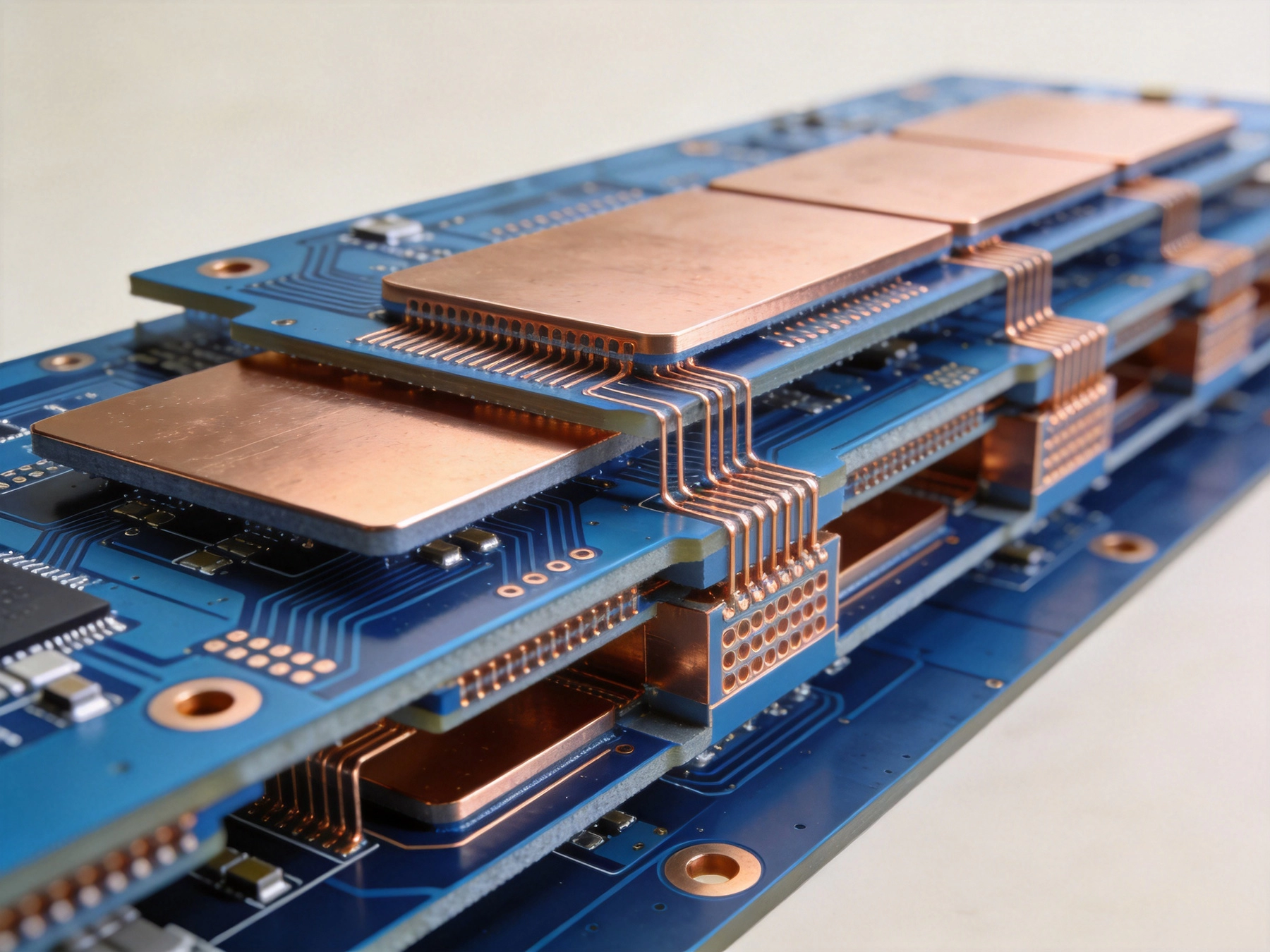
Signal integrity encompasses the study and management of electrical signal quality as it propagates through PCB interconnects. At low frequencies, virtually any copper trace can conduct signals adequately. However, as signal edge rates increase and data rates climb into the hundreds of megahertz and beyond, the physical characteristics of interconnects become significant. Transmission Line effects, impedance discontinuities, and electromagnetic coupling all manifest in ways that degrade signal quality if not properly managed.
Characteristic impedance represents the most fundamental signal integrity parameter, describing the apparent impedance of a Transmission Line as seen by a propagating signal. When the characteristic impedance of a trace matches the source and load impedances, maximum power transfer occurs and reflections are minimized. Deviations from this matched condition cause portions of the signal to reflect back toward the source, creating standing waves, ringing, and timing errors that corrupt data and reduce noise margins.
Return current paths determine how signals couple to reference planes and influence both radiated emissions and susceptibility to external interference. At low frequencies, current returns through the path of lowest resistance. At high frequencies, however, current follows the path of lowest impedance, which means it flows directly beneath the signal trace on the nearest reference plane. This高频 behavior makes reference plane continuity critical; gaps, slots, or vias that interrupt return current paths create impedance discontinuities and increase electromagnetic radiation.
Higher layer counts directly enable improved signal integrity through expanded access to reference planes and more sophisticated layer stacking strategies. A four-layer board offers limited options for referencing and shielding, often forcing designers to route high-speed signals adjacent to sparse or fragmented reference planes. Six-layer boards begin to provide adequate reference plane coverage, but eight layers or more enable the sophisticated stacking arrangements that fully address signal integrity requirements for demanding applications.
The availability of dedicated power and ground planes in high-layer count designs enables capacitor placement strategies that maintain low impedance power delivery across the frequency spectrum. Decoupling capacitors must be positioned close to IC power pins and connected through short, low-inductance paths to nearby power and ground planes. With adequate layers, these connections can be optimized, and the plane structure itself provides the high-frequency capacitance that supplements discrete capacitors.
Shielding between signal layers becomes possible with sufficient layer counts, reducing crosstalk between adjacent routing channels. By allocating complete layers to shielding functions, designers can isolate sensitive signal groups from noisy ones without sacrificing routing density. This isolation capability proves particularly valuable in mixed-signal designs where analog and digital circuits must coexist without mutual interference.
High-density interconnect technology represents a collection of manufacturing techniques that enable finer geometries, higher densities, and more sophisticated structures than conventional PCB processes. Core HDI capabilities include microvia formation using Laser Drilling, Sequential Lamination that enables complex layer stacking, and fine-line routing that achieves significantly higher routing density than standard processes. These capabilities directly address the signal integrity challenges that arise at modern data rates.
Microvias constitute the defining feature of Hdi Technology, offering substantial advantages over mechanically drilled through-holes. With diameters measured in tens or hundreds of microns rather than hundreds of microns, Microvias introduce minimal discontinuities in signal paths. Their depth-to-diameter ratios are carefully controlled, and they can be placed directly adjacent to component pads, enabling shortest-possible connections that minimize parasitic inductance and radiation.
Sequential Lamination enables the construction of complex multilayer structures that would be impossible with conventional processes. By building up boards in multiple stages, designers can create interleaved layer structures with multiple thin dielectric layers between reference planes. This capability enables Impedance Control strategies and shielding arrangements that dramatically improve signal integrity for the most demanding applications.
The geometry of traditional through-hole vias creates significant signal integrity problems, particularly at high frequencies. The long barrel of a through-hole acts as a transmission line stub that resonates at certain frequencies, creating notch filters in the frequency response and introducing ringing in time-domain signals. The pad and antipad structures required for through-holes also increase capacitance at the via, further degrading signal quality.
Microvias address these problems through their minimal geometry. The short length of microvias, combined with their small diameter, creates structures with extremely low parasitic inductance and capacitance. When properly designed, microvia transitions approach the ideal connection between layers, with minimal impedance discontinuity. This capability enables high-speed interfaces to transition between layers without the signal degradation that through-hole vias introduce.
Via-in-pad technology, wherein microvias are placed directly in component pads, represents the ultimate in low-inductance connections. By eliminating the stub entirely and connecting directly from the component pad to the internal layer, Via-in-pad structures provide the cleanest possible electrical connection. This technique requires sophisticated manufacturing capabilities and careful design attention to avoid manufacturing defects, but the signal integrity benefits justify the additional complexity for critical applications.
Reference plane design establishes the foundation upon which signal integrity is built in multilayer PCBs. Every high-speed signal requires a reference plane that provides return current path and defines the transmission line environment. The quality, continuity, and proximity of these reference planes directly determine achievable signal integrity performance. Understanding reference plane requirements enables designers to specify layer stacks and routing strategies that support demanding applications.
Plane continuity ranks among the most critical reference plane requirements. Return current must be able to follow the signal trace without encountering obstacles that force it to detour around planes. Vias that must pass through reference planes require antipads that create gaps in the reference, forcing return current to flow around these openings. When multiple signals pass through the same via, their return currents can interact, creating additional crosstalk. Careful via placement that groups signals sharing the same reference minimizes these interactions.
Reference plane selection influences both signal integrity and radiated emissions. Signals referenced to solid planes experience consistent impedance determined by the dielectric geometry. Signals referenced to split planes, where different voltage domains occupy different regions, encounter impedance variations at plane boundaries. While split planes can isolate power domains, they create discontinuities that must be carefully managed for high-speed signals.
High-layer count designs enable sophisticated power delivery networks that maintain stable voltages despite transient current demands from processors, FPGAs, and other high-power components. The impedance of the Power Distribution system determines how effectively voltage variations are suppressed, with lower impedance enabling cleaner power delivery. PDN design directly affects signal integrity because supply noise modulates the reference voltages against which signals are interpreted.
Decoupling strategy for high-speed circuits must address multiple frequency ranges, from kilohertz through tens of gigahertz. Bulk capacitors handle low-frequency variations with their larger values but higher ESR and ESL. Mid-frequency decoupling relies on smaller capacitors with lower parasitic values. High-frequency decoupling depends on the intrinsic capacitance of power and ground planes separated by thin dielectrics. High-layer count boards enable all three strategies through proper layer assignment and capacitor placement.
Voltage regulator module placement influences PDN performance significantly. VRMs positioned far from load devices introduce series inductance that degrades high-frequency response. With adequate routing layers, VRMs can be placed close to loads, with power delivered through wide traces or planes that minimize impedance. For the highest-performance applications, embedded voltage regulation within the PCB structure eliminates the distance problem entirely.
Controlled Impedance traces provide the consistent transmission line environment that high-speed signals require for reliable communication. Achieving controlled impedance requires careful attention to trace geometry, dielectric properties, and the geometry of adjacent reference structures. High-layer count boards enable controlled impedance routing through precise control of trace dimensions and dielectric spacing, making Impedance Control practical across entire designs rather than limited to critical nets.
Microstrip and Stripline geometries each offer advantages for controlled impedance implementation. Surface Microstrip traces on outer layers achieve impedance based on trace width, copper thickness, and the Dielectric Constant and thickness of the surrounding material. Stripline traces embedded between reference planes experience more complex field distributions but offer shielding that reduces emissions and susceptibility. High-layer count designs can implement both geometries as appropriate for different signal types.
Differential pair routing requires additional consideration beyond single-ended impedance control. The differential impedance depends on trace width, spacing, and the dielectric environment, with tight coupling maximizing common-mode noise rejection. High-layer count boards enable Differential Pairs to maintain consistent coupling throughout their routing, with reference planes providing consistent environment even as trace geometry varies with routing constraints.
Impedance tolerances reflect both design requirements and manufacturing capabilities, with tighter tolerances requiring more sophisticated processes and more careful control. Typical impedance tolerances range from ±10% for standard commercial products to ±5% for demanding applications. The most sensitive high-speed interfaces may require ±3% or tighter tolerances, achievable only with premium manufacturing processes and careful verification through impedance testing.
Manufacturing process variation influences achievable impedance tolerances significantly. Dielectric Constant variation in substrate materials, trace width variation in etching processes, and plating thickness variation all contribute to impedance uncertainty. High-layer count boards benefit from more stable manufacturing environments and tighter process controls that enable more consistent impedance. However, design practices must still account for reasonable manufacturing variation to ensure acceptable yields.
Impedance testing and verification confirm that manufactured boards meet design intent. Time-domain reflectometry provides direct measurement of trace impedance and can identify the location of impedance discontinuities. Test coupons on production panels enable statistical process control that tracks impedance capability over time. This verification investment is essential for high-speed designs where marginal impedance control can cause field failures.
Crosstalk, the unwanted coupling of signals between adjacent traces, becomes increasingly problematic as board densities increase. At low frequencies, crosstalk depends primarily on capacitive and inductive coupling coefficients. At high frequencies, however, crosstalk also involves wave propagation effects that can extend coupling over significant distances. Managing crosstalk requires attention to trace geometry, separation, and shielding throughout the design.
Trace spacing directly affects crosstalk levels, with greater separation reducing coupling. The 3W rule, which spaces traces by three times their width, provides approximately 70% crosstalk reduction compared to adjacent traces. The 5W rule achieves approximately 90% reduction. High-layer count designs provide the routing resources that enable these separations for critical signals without sacrificing overall routing density for less sensitive nets.
Layer assignment for sensitive signals affects crosstalk through the field distributions that neighboring layers create. Stripline traces between solid reference planes experience minimal coupling to traces on adjacent layers because reference planes shield the field interactions. Surface microstrip traces couple more strongly to traces on adjacent layers, requiring additional separation or routing on orthogonal layers to manage crosstalk.
Dedicated shielding layers isolate critical signals from interference and reduce their emissions. By routing sensitive signals between solid reference planes, shielding provides both electric and magnetic field containment. This technique requires multiple layers and sophisticated routing but achieves crosstalk levels unattainable through spacing alone. High-layer count designs enable this approach for all critical signals, not just those in special locations.
Guard traces placed between aggressive and sensitive signals provide intermediate isolation. Connected to the reference plane at regular intervals through stitching vias, guard traces absorb coupling currents and return them to ground. This technique is particularly valuable for coupling reduction between traces on the same layer where spacing cannot be increased sufficiently. Guard traces consume routing space but enable higher-density implementations than spacing alone would allow.
Differential signaling provides inherent common-mode rejection that reduces susceptibility to crosstalk. Because crosstalk typically couples equally to both members of a differential pair, it appears as common-mode noise that the differential receiver rejects. This advantage makes differential signaling attractive for high-speed interfaces, particularly when combined with the tight coupling that differential routing requires.
Electromagnetic interference emissions from PCBs are governed by both the signals they carry and the structures that contain them. High-layer count designs with proper reference planes act as transmission line waveguides that contain electromagnetic fields, reducing both emissions and susceptibility. Conversely, inadequate reference planes and uncontrolled routing create antennas that radiate efficiently, causing regulatory compliance failures and system interference problems.
Return current path integrity directly affects emissions because interrupted return paths force current to find alternate routes that typically involve larger loops. These larger loops radiate more efficiently, increasing both emissions and susceptibility. By ensuring continuous reference planes and minimizing plane discontinuities, high-layer count designs reduce the antenna efficiency of signal routing.
Edge plating and shielding techniques in high-layer count designs further reduce emissions by containing fields at board edges. Uncontrolled edges allow fields to radiate from the perimeter of the board, while properly terminated edges prevent this radiation. These techniques are particularly important for boards operating in electrically noisy environments or those subject to stringent regulatory emission limits.
Grounding philosophy influences EMI performance significantly, with different approaches suitable for different applications. Single-point grounding works for low-frequency circuits but creates ground loops at high frequencies. Multi-point grounding maintains low impedance to reference planes at high frequencies but can create ground loops at lower frequencies. Understanding these tradeoffs enables selection of grounding approaches matched to the frequency content of signals being routed.
Via stitching connects reference planes at multiple points, reducing plane impedance and preventing differential voltages from developing between different regions of the same plane. Stitching via density should be adequate for the highest frequency of concern, with spacing of one-tenth wavelength or less between stitching vias. High-layer count boards provide the routing access to implement dense stitching where needed.
Slot openings in reference planes create discontinuities that affect both signal integrity and emissions. Slots that interrupt return current paths force current to flow around the opening, increasing loop area and radiation. When slots cannot be avoided, stitching vias around slot boundaries help contain fields and reduce the radiation from slot antennas.
Successful high-speed Pcb Design requires systematic attention to signal integrity from initial architecture through final verification. Design guidelines encode lessons learned from previous designs and provide frameworks that help engineers avoid common mistakes. While specific guidelines vary by application and data rate, underlying principles remain consistent across designs.
Layer stack design establishes the foundation for signal integrity performance. The stack should provide adequate reference planes, appropriate dielectric thicknesses for impedance control, and sufficient separation between high-speed signal layers and noisy power layers. High-layer count designs offer flexibility to optimize the stack for specific application requirements rather than accepting generic configurations.
Pin assignment and breakout routing from high-pin-count devices critically influence signal integrity for the most demanding interfaces. BGA packages with hundreds or thousands of pins require careful planning to ensure that critical signals reach reference planes promptly after leaving the device. HDI technology enables escape routing patterns that minimize stub lengths and maintain reference continuity throughout the fanout region.
Signal integrity verification should begin with simulation during design and continue through measurement during prototyping. IBIS models extracted from component characteristics enable simulations that predict performance before boards are manufactured. These simulations identify potential problems while design changes remain inexpensive, avoiding costly respins of finished boards.
Time-domain reflectometry and time-domain transmission measurements on prototype boards verify that actual performance matches predictions. Unexpected reflections or crosstalk indicate design or manufacturing issues that require investigation. Resolution of these issues informs design guidelines for future projects, building organizational expertise in high-speed design.
Compliance testing for regulatory emissions and susceptibility confirms that designs meet external requirements. Pre-compliance testing during development identifies issues before formal testing, reducing the risk of certification delays. High-layer count and HDI designs that follow good signal integrity practices typically achieve compliance more readily than designs that treat these issues as afterthoughts.
Signal integrity requirements continue escalating as data rates push toward terabit-per-second speeds in emerging applications. This progression drives adoption of ever-more-sophisticated PCB technologies, including advanced HDI structures, embedded passives, and optical interconnects integrated with electrical PCBs. Designers must understand these emerging capabilities to position their products for future requirements.
Embedded component technology promises significant signal integrity improvements by eliminating discrete components entirely. Resistors, capacitors, and even inductors embedded within PCB layers eliminate the parasitic inductance and capacitance of surface-mount devices. While manufacturing complexity currently limits adoption, embedded passives offer advantages that will drive increasing use in demanding applications.
Photonics integration with PCBs represents the frontier of signal integrity, enabling optical interconnects that eliminate the loss and dispersion limitations of copper at ultra-high speeds. While fully optical PCBs remain experimental, hybrid solutions that combine optical and electrical interconnect on the same substrate are entering production for data center and telecommunications applications. These technologies will shape signal integrity practice for the most advanced systems.
Q: What is the minimum layer count for effective High-speed Pcb design?
A: While requirements vary by application, six layers typically represent the minimum for adequate high-speed design with controlled impedance, power integrity, and routing resources. Eight layers or more enable more sophisticated approaches that address demanding applications. The specific minimum depends on signal speeds, component densities, and whether HDI features are required.
Q: When should HDI technology be specified for signal integrity?
A: HDI becomes beneficial when component packages require fine-pitch routing, when via stub effects limit performance at high frequencies, when routing density prevents adequate spacing on conventional layers, or when smallest-possible trace widths and spacings are needed for controlled impedance. HDI adds manufacturing cost, so the benefits must justify this investment.
Q: How do I determine appropriate impedance tolerances for my design?
A: Impedance tolerance requirements derive from signal margin analysis for the specific interfaces being implemented. Higher-speed interfaces with tighter margins require tighter impedance control. As a starting point, ±10% suffices for moderate-speed signals, ±7% for DDR interfaces, and ±5% or tighter for the fastest serial links. Consult interface specifications for specific requirements.
Q: What is the impact of via stubs on signal integrity?
A: Via stubs act as transmission line resonators that create notch filters in frequency response and ringing in time-domain signals. Stub resonances occur at frequencies where the stub length equals one-quarter wavelength. For high-speed signals, stubs can cause significant eye degradation at frequencies well within the signal bandwidth. Back-drilling or HDI microvias eliminate stubs for critical signals.
Q: How can I verify signal integrity in my design before manufacturing?
A: Signal integrity simulation using IBIS or SPICE models predicts performance based on design geometry. Tools that extract transmission line parameters from PCB data enable accurate modeling of routing effects. Correlation of simulation results with measurements on similar designs validates the modeling approach and builds confidence in predictions.
Signal integrity has evolved from a specialized concern for a few advanced applications to a fundamental requirement for virtually all electronic products. High-layer count PCBs and HDI technology provide the capabilities necessary to achieve the signal integrity performance that modern applications demand. By enabling proper reference planes, controlled impedance routing, and microvia structures, these technologies address signal integrity at the physical layer rather than requiring compensation through higher protocol margins.
The benefits of high-layer count and HDI solutions extend beyond basic signal integrity to encompass reduced emissions, improved immunity, and more compact implementations. These advantages compound through the product development process, enabling faster design cycles, higher first-pass success rates, and more robust field performance. While these technologies introduce additional complexity and cost, their benefits typically justify the investment for products where signal integrity matters.
As data rates continue increasing and electronic systems become ever more integrated, the importance of signal integrity expertise will only grow. Designers who master the principles outlined in this article position themselves to create products that perform reliably in increasingly demanding electromagnetic environments. The investment in understanding high-layer count and HDI technologies returns dividends across the product lifecycle, from initial development through long-term field support.
Material Selection Guide for High-Speed Industrial PCB SolutionsJuly/14/2026
Aluminum vs. Copper Base: Choosing the Best Metal Core SolutionJuly/29/2026

Innovative Industrial PCB Solutions for Renewable Energy SystemsAugust/10/2026
Heavy Copper PCBs: The Solution for High-Current Industrial ApplicationsJune/18/2026
Manufacturing Processes Unique to Rigid-Flex PCB SolutionsOctober/10/2026
Manufacturing Challenges in 20+ Layer Industrial PCB SolutionsJuly/09/2026

Tailored Industrial PCB Solutions for Medical Device ManufacturersJune/12/2026
An Introduction to HDI Technology for Compact Industrial ElectronicsJune/16/2026