Open Nav


High-end industrial PCB Fabrication demands tolerances that would seem impossible to manufacturers focused on consumer electronics. In applications ranging from aerospace navigation systems to medical imaging equipment, from precision motor controls to defense electronics, the difference between meeting and missing tolerance specifications can determine system performance, safety, and reliability. Precision engineering in PCB Fabrication extends far beyond simple dimensional accuracy—it encompasses a comprehensive understanding of how material properties, manufacturing processes, environmental conditions, and design decisions interact to influence final product characteristics. Manufacturers who excel at tight tolerance control deliver components that enable systems to perform at levels impossible with standard tolerances. This comprehensive exploration of tolerances in high-end Industrial Pcb fabrication provides insights into the engineering principles, manufacturing capabilities, and quality systems that enable precision Electronics Manufacturing for the most demanding applications.
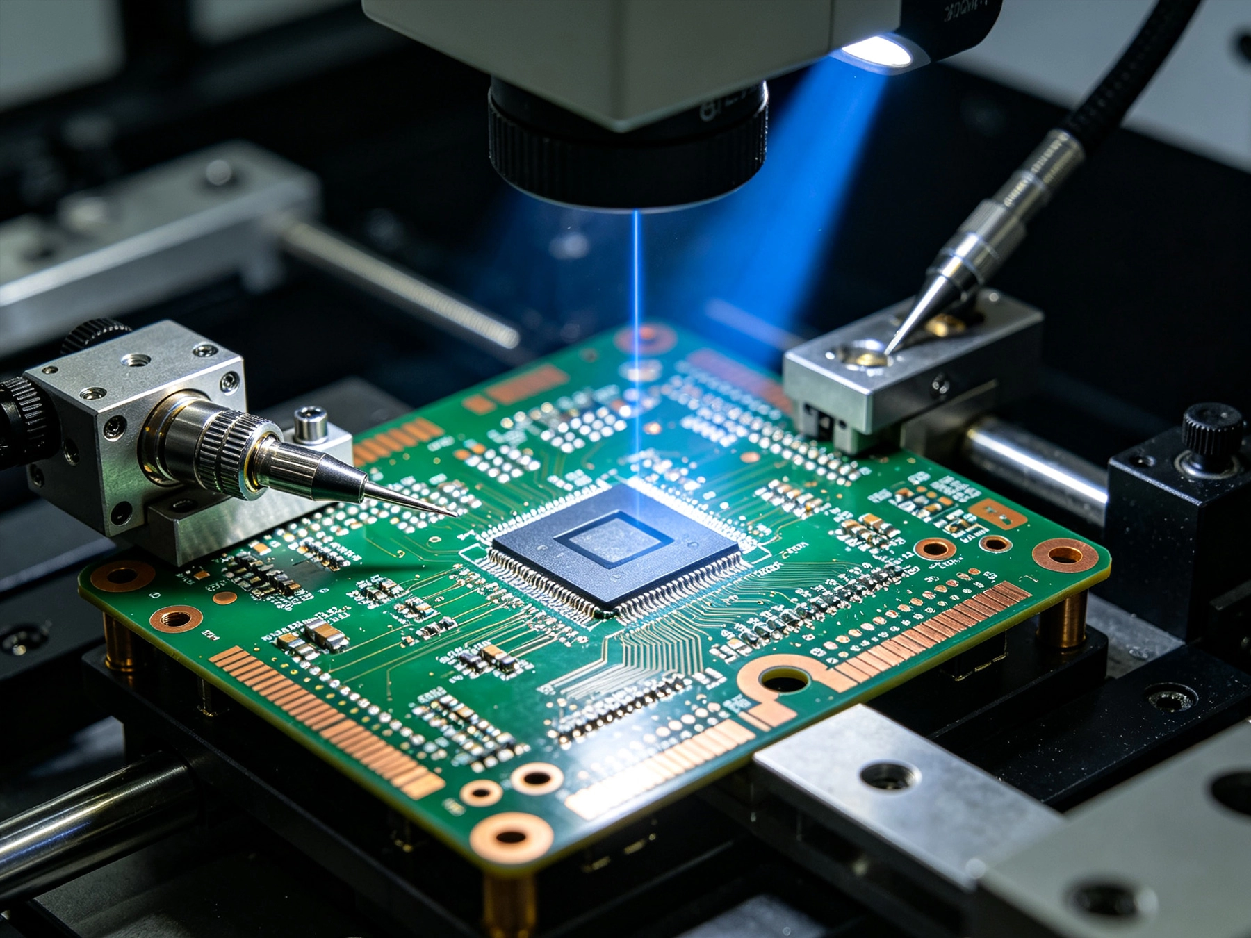
Tolerance in Pcb Fabrication refers to the acceptable range of deviation from specified dimensions or characteristics. Every manufacturing process introduces some variation, and tolerance specifications define the acceptable limits of that variation. In high-end industrial applications, tolerances must be sufficiently tight to ensure consistent electrical performance, mechanical fit, and functional reliability while accounting for variations in materials, processes, and environmental conditions. Dimensional tolerances address physical dimensions including board thickness, trace width, drill diameter, and hole position. These directly impact manufacturing yield and cost, creating pressure to specify tolerances as loosely as possible. However, electrical tolerances including Impedance Control, capacitance, and inductance values may demand tighter dimensional control to achieve required electrical performance. Material tolerances address variations in substrate properties, copper weight, and prepreg characteristics that influence both electrical and mechanical performance. Process tolerances define acceptable variations in plating thickness, Solder Mask coverage, and surface finish quality. Understanding the relationships between these different tolerance types enables designers to specify tolerances that ensure functional requirements while avoiding unnecessary manufacturing cost and complexity.
Modern Pcb Fabrication equipment achieves remarkable dimensional precision, but absolute limits exist based on material properties, process physics, and economic constraints. Board thickness tolerances typically range from ±10% for standard boards down to ±5% for controlled thickness boards and ±3% for precision applications. Standard substrate materials including FR-4 exhibit thickness variations of 5-10% across a single panel due to glass weave distribution and resin flow during lamination. Achieving tighter thickness tolerances requires specialized materials, enhanced process control, and sometimes in-process measurement and selection. Trace width tolerances for standard production typically run ±20% for outer layers and ±15% for inner layers. High-precision processes can achieve ±10% or better, with some specialized manufacturers claiming ±5% under ideal conditions. Trace width tolerance represents a particular challenge because etching processes naturally produce some variation, and trace width directly impacts impedance in high-frequency applications. Drill diameter tolerances for plated holes typically run ±0.05mm to ±0.10mm depending on drill size and plating requirements. Blind and Buried Via tolerances are tighter due to the complexity of layer-to-layer registration. Hole position tolerances range from ±0.10mm for standard through-holes to ±0.025mm for precision applications requiring sophisticated registration systems and statistical process control.
Layer registration—the precision with which holes and features on different layers align—represents one of the most challenging tolerance aspects in Multilayer Pcb fabrication. As layer count increases and feature density grows, registration tolerances become increasingly critical. Standard multilayer registration typically achieves ±0.10mm to ±0.15mm depending on board complexity and manufacturer capability. High-precision multilayer processes can achieve ±0.05mm registration through advanced imaging systems,strict process controls, and sophisticated registration targets. Blind and Buried Via structures require even tighter control because layer-to-layer misregistration directly impacts electrical connectivity and reliability. The fundamental challenge involves managing material behavior during lamination, where thermal expansion and resin flow cause dimensional changes that vary with board construction, layer count, and press parameters. Sophisticated manufacturers use statistical process control to monitor and adjust for material variations, maintaining registration within specification despite inherent process variability. Automated optical inspection systems measure registration at multiple points across each panel, enabling real-time process adjustment and statistical analysis of capability. For the most demanding applications, some manufacturers perform 100% inspection of registration parameters, rejecting any panels that exceed tolerance limits.
Electrical tolerances in high-end industrial PCBs often drive the tightest dimensional requirements, particularly for high-speed digital and RF applications. Impedance tolerance specifications typically range from ±10% for standard Controlled Impedance boards to ±5% for precision applications and ±2% for the most demanding high-frequency applications. Achieving ±5% impedance tolerance requires controlling trace width to approximately ±5%, dielectric thickness to approximately ±3%, and material Dielectric Constant to approximately ±2%. These requirements cascade through the entire manufacturing process, demanding tight control of etching parameters, lamination pressure and temperature, and material specifications. Transmission Line tolerances for 50-ohm and other characteristic impedances depend on trace geometry, dielectric properties, and return path configuration. Coupled line structures used for differential signaling require additional controls on spacing between traces, as differential impedance depends on both individual trace impedance and coupling between traces. Capacitance tolerances for high-frequency filters and matching networks may demand extremely tight control of trace dimensions and dielectric properties. Advanced manufacturers use test coupons, time-domain reflectometry, and vector network analysis to verify impedance characteristics on every production panel, ensuring electrical performance meets specifications before subsequent assembly operations.
Material Selection significantly influences achievable tolerance in high-end PCB fabrication. Standard FR-4 materials exhibit Dielectric Constant variations of ±5-10% between batches and within sheets, making tight Impedance Control challenging. High-performance materials including polyimide, Rogers laminates, and ceramic-filled substrates offer more consistent properties and tighter tolerance capability. Thermoset polyimide materials provide excellent dimensional stability during processing and wide operating temperature ranges, making them suitable for aerospace and industrial applications. Filled materials including ceramic-filled PTFE offer consistent dielectric properties and low loss characteristics for RF applications. Reinforcement selection influences dimensional stability, with spread glass weaves reducing thickness variation compared to conventional woven glass. Pressing parameters must be optimized for each material combination, as different resins exhibit different flow characteristics and cure kinetics. Some manufacturers specify materials to narrower property ranges than standard datasheet values, performing incoming inspection and selective sourcing to ensure material consistency. For the most demanding applications, material certification including dielectric constant verification and lot traceability becomes mandatory.
Achieving tight tolerances consistently requires sophisticated process control and continuous capability analysis. Statistical process control monitors key parameters throughout manufacturing, using control charts to identify trends and trigger corrective actions before out-of-tolerance conditions occur. Process capability indices including Cp and Cpk quantify the ability of processes to meet specifications, with high-end manufacturers targeting Cpk values above 1.33 for critical parameters. Process capability improvement requires understanding variation sources and systematically reducing them through equipment upgrades, environmental controls, and procedure optimization. Environmental factors including temperature, humidity, and vibration influence manufacturing precision, particularly for imaging and drilling operations. Climate-controlled facilities maintain stable environmental conditions that enable consistent processing. Equipment calibration schedules ensure measuring instruments provide accurate data for process control decisions. Operator training and certification programs ensure consistent execution of critical procedures. Documentation and traceability systems capture process parameters for every panel, enabling root cause analysis when issues occur and Continuous Improvement across production runs.
Precision tolerance verification requires sophisticated inspection methods beyond simple dimensional measurement. Automated optical inspection systems measure trace widths, spacings, and registration with resolutions approaching 1 micron, enabling comprehensive panel-level characterization. X-ray Inspection examines internal structures including vias, internal layers, and plating quality without destructive sectioning. Cross-sectional analysis provides detailed information about plating thickness, dielectric dimensions, and structural integrity for qualification and Failure Analysis. Electrical testing including open/short verification, netlist validation, and impedance measurement confirms electrical characteristics meet specifications. For high-frequency applications, time-domain reflectometry and network analysis provide detailed electrical characterization beyond simple continuity testing. Optical coordinate measuring systems verify hole positions and mechanical dimensions with precision exceeding 10 microns. Scanning acoustic microscopy detects Delamination, voids, and other internal defects that might not be visible externally. The combination of these inspection methods provides comprehensive assurance that precision requirements are met, though inspection costs contribute significantly to total manufacturing expense.
Successful precision PCB fabrication requires collaborative design practices that balance functional requirements with manufacturing capabilities. Design rule checking verifies that specified tolerances fall within manufacturer capability ranges, preventing specification of tolerances that cannot be consistently achieved. Communication between designer and manufacturer early in the design process enables optimization of tolerance specifications based on actual manufacturing capabilities. Balanced tolerance stacks analyze cumulative effects of multiple tolerance contributions, preventing situations where individual tolerances are achievable but combined effects exceed requirements. Worst-case analysis and statistical tolerance analysis provide different insights into design robustness, with statistical methods often revealing that looser individual tolerances can achieve equivalent system performance. Feature grouping strategies concentrate tight tolerance features in areas where manufacturing control is easiest, avoiding scattered tight requirements that increase complexity. Panel utilization optimization may influence tolerance capability, as panel edge effects and panel-to-panel variations differ from within-panel variations. Prototype builds enable validation of tolerance achievement before committing to production, providing opportunity for specification refinement based on actual results.
Precision tolerances inevitably increase manufacturing cost, making cost-benefit analysis essential for tolerance specification. Tooling costs including drilling programs, imaging films, and inspection templates represent fixed investments that spread across production volume. Process complexity increases with tighter tolerances, requiring more sophisticated equipment, tighter environmental controls, and more extensive inspection. Yield rates typically decrease as tolerance requirements tighten, as the acceptable window for each parameter shrinks. Material costs for high-performance substrates often exceed standard material costs by factors of 2-5, depending on specific materials and availability. Inspection intensity increases for precision applications, with 100% inspection replacing statistical sampling in some cases. Engineering time for process development and qualification adds to non-recurring costs that must be amortized across production volume. The cost premium for precision tolerance varies by complexity level but typically ranges from 20-50% for moderately tight tolerances to 100-200% for the most demanding precision requirements. Understanding the sources of precision cost premium enables informed decisions about where tight tolerances are truly necessary versus where standard tolerances would suffice.
Different industrial applications impose different tolerance requirements based on functional needs and operating conditions. Aerospace applications demand tight tolerances for reliability in extreme environments, with military specifications often requiring detailed tolerance documentation and statistical process capability data. Medical electronics require tolerances that ensure safety and efficacy, with regulatory requirements driving documentation and traceability needs. Industrial control systems demand tolerances that ensure consistent performance over extended operating lifetimes in harsh environments. Defense electronics may require tolerances supporting specialized packaging and interconnection approaches including chip-on-board and multi-chip modules. Automotive Electronics increasingly demand precision for safety-critical systems including ADAS and autonomous driving. The trend toward higher-frequency applications including 5G, radar, and satellite communications drives increasingly tight impedance tolerance requirements. Understanding application-specific requirements enables appropriate tolerance specification that ensures functional requirements are met without unnecessary cost premium for specifications beyond actual needs.
Precision tolerance capabilities continue advancing as manufacturing technologies evolve. Direct imaging systems replace photographic imaging, enabling tighter feature placement and reduced registration error. Advanced materials including ultra-low loss substrates and engineered dielectrics provide more consistent electrical properties. Additive manufacturing techniques including 3D-printed substrates and embedded traces enable novel structures that bypass traditional tolerance limitations. In-process metrology provides real-time feedback that enables closed-loop control of critical parameters, improving consistency and reducing variation. Artificial intelligence and machine learning analyze manufacturing data to identify optimization opportunities and predict quality outcomes before inspection completes. Panel-level processing advances enable larger panels with improved uniformity, reducing within-panel variation that contributes to tolerance stack-up. Embedded component technologies integrate passives and actives within PCB structures, potentially reducing sensitivity to some external tolerances. These advances will continue pushing the boundaries of achievable precision while hopefully reducing costs through improved process efficiency and yield rates.
Precision engineering tolerances in high-end Industrial Pcb fabrication represent a sophisticated interplay between design requirements, material science, manufacturing technology, and quality systems. Achieving tight tolerances consistently requires understanding the fundamental limits imposed by materials and processes while implementing rigorous controls that minimize variation within those limits. The investment in precision tolerance capability—through advanced equipment, sophisticated process controls, comprehensive inspection, and highly trained personnel—enables manufacturing of PCBs that power the most demanding electronic applications. As electronic systems continue pushing performance boundaries in communications, computing, medical, aerospace, and industrial applications, the importance of precision tolerance control will only increase. Manufacturers who invest in precision capability position themselves to serve the most demanding applications and contribute to advancement across industries where electronic performance directly impacts safety, reliability, and capability. For design engineers, understanding tolerance fundamentals and manufacturing capabilities enables specification of tolerances that achieve functional requirements while minimizing unnecessary cost premium for precision beyond actual needs.
What tolerances can high-end PCB manufacturers achieve?
High-end PCB manufacturers typically achieve trace width tolerances of ±10-15% for standard processes and ±5% for precision processes. Hole diameter tolerances range from ±0.05mm to ±0.10mm depending on hole size. Hole position tolerances can reach ±0.025mm to ±0.05mm for precision multilayer boards. Impedance tolerances from ±10% for standard Controlled Impedance down to ±2% for the most demanding high-frequency applications. Thickness tolerances from ±10% standard to ±3% for precision applications. The specific achievable tolerances depend on board complexity, layer count, and manufacturer capability.
How do tight tolerances affect Pcb Manufacturing cost?
Tight tolerances increase manufacturing cost through several mechanisms: more sophisticated equipment with tighter control capabilities, enhanced environmental controls for temperature and humidity stability, increased inspection intensity including 100% testing instead of sampling, reduced yields as acceptable windows shrink, higher-performance materials with more consistent properties, and additional engineering time for process development and qualification. Cost premiums typically range from 20-50% for moderately tight tolerances to 100-200% for the most demanding precision requirements.
What drives impedance tolerance requirements in PCBs?
Impedance tolerance requirements are driven by Signal Integrity requirements in high-speed digital applications and RF/microwave requirements in wireless communications. Faster signal edges and higher frequencies reduce acceptable impedance mismatch, requiring tighter tolerance to maintain signal quality. Differential signaling applications often require tight tolerances on both individual trace impedance and differential impedance. Long transmission lines accumulate more reflection damage, requiring tighter impedance control. Impedance-sensitive applications include 5G communications, radar systems, high-speed data links, and precision measurement equipment.
How do material variations affect achievable tolerances?
Material variations significantly impact achievable tolerances, particularly for electrical applications. Standard FR-4 exhibits dielectric constant variations of ±5-10% between batches and within sheets, making tight impedance control challenging. Glass weave distribution creates thickness variations of 5-10% across panels. Copper roughness variations affect effective dielectric thickness. High-performance materials including polyimide and Rogers laminates offer more consistent properties but at higher cost. Material Selection and incoming inspection become critical for precision applications where material variations directly impact electrical performance.
What inspection methods verify precision tolerances?
Precision tolerance verification uses multiple inspection methods: automated optical inspection (Aoi) for trace widths, spacings, and registration with micron resolution, X-ray Inspection for internal structures and plating quality, cross-sectional analysis for detailed dimensional verification, electrical testing including TDR for impedance measurement, coordinate measuring machines for mechanical dimensions, and scanning acoustic microscopy for internal defects. The combination of these methods provides comprehensive assurance that precision requirements are met, though inspection intensity significantly contributes to total manufacturing cost.
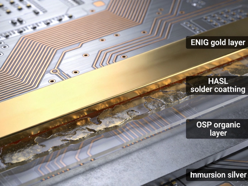
The Impact of Surface Finishes on Industrial PCB Fabrication QualityJuly/16/2026
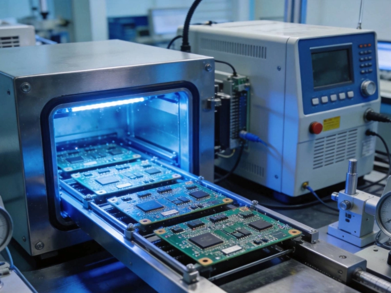
Predicting Lifespan: Accelerated Life Testing for Industrial PCB ReliabilityAugust/03/2026

Eco-Friendly Practices in Modern Industrial PCB FabricationSeptember/20/2026
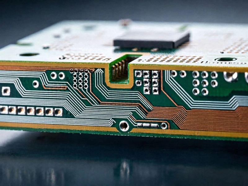
Advanced Techniques in Multi-Layer Industrial PCB FabricationJune/03/2026
Materials, Methods, and Industry Standards ExplainedMay/27/2026

Overcoming Common Defects in Industrial PCB FabricationAugust/03/2026

How to Choose the Right Manufacturer for Industrial PCB FabricationJune/29/2026
The Role of Laser Drilling in High-Precision Industrial PCB FabricationOctober/15/2026