Open Nav


Industrial Pcb applications place unique demands on substrate materials that do not exist in consumer or commercial electronics. High-speed digital communication systems for Industrial Automation must maintain Signal Integrity across extended temperature ranges and long operational lifecycles. High-power Power Electronics for motor drives and renewable energy systems must dissipate significant heat while maintaining electrical isolation between high-voltage circuits. High-frequency RF systems for industrial sensing and communication must deliver consistent performance across years of operation in harsh environments. Two material properties define whether a Pcb Substrate can meet these challenging requirements: Dielectric Constant and loss tangent. Understanding what these properties mean, how they interact with design requirements, and how they vary across different material families is essential for any engineer designing Industrial Electronics.
Too often, industrial designers treat these properties as afterthoughts, using generic values from datasheets without accounting for how they change with frequency, temperature, and manufacturing variation. This oversight leads to designs that perform well in simulation but fail in real-world industrial environments, resulting in costly redesigns, delayed product launches, and field failures that erode customer trust. By building a practical understanding of Dielectric Constant and loss tangent, engineers can select materials that meet performance requirements while optimizing for cost, manufacturability, and long-term reliability.
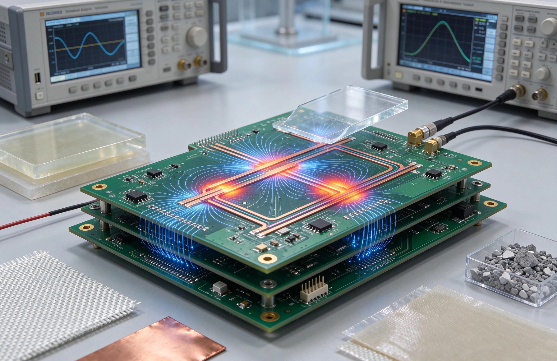
Dielectric constant, also called relative permittivity and often abbreviated as Dk or εr, describes how a dielectric material affects the electric field between two conductors. When an electric field is applied across a dielectric material, the molecules within the material polarize, reducing the effective electric field for a given applied voltage compared to the same field in a vacuum. The dielectric constant is the ratio of the capacitance between two conductors separated by the dielectric material to the capacitance of the same conductors separated by a vacuum. A higher Dk means the material stores more electric charge per unit voltage, increasing the effective capacitance between conductors.
The most direct impact of Dk on Pcb Design is its effect on Transmission Line impedance and signal propagation velocity. For a Microstrip Transmission Line with fixed trace width and height above the reference plane, a higher Dk will produce a lower characteristic impedance. Designers adjust trace geometry to compensate for different Dk values to achieve the target impedance, typically 50 ohms for RF applications or 90/100 ohms for high-speed Differential Pairs. The propagation velocity of signals through the transmission line is inversely proportional to the square root of Dk: higher Dk means slower signal propagation, which directly affects timing budgets in high-speed digital designs.
Dk is not a fixed property for any material. It varies with frequency, temperature, humidity, and material composition. Most Pcb Substrate materials show relatively stable Dk at low frequencies, but many exhibit significant variation as frequencies rise into the gigahertz range. This frequency dependence, called dielectric dispersion, means that the Dk value specified at 1 MHz on a datasheet may be significantly different from the actual Dk at 10 GHz. For high-frequency or high-speed industrial designs, using the Dk value measured at the actual operating frequency is critical for accurate impedance calculations and Signal Integrity simulation.
Material consistency and Dk tolerance are also critical for industrial applications. Datasheet values typically report nominal Dk, but actual material production lots may vary within a specified tolerance range. Standard FR4 materials may have Dk tolerances of ±0.15 or more, while high-performance materials designed for high-frequency applications may offer tolerances as tight as ±0.05. For designs with tight impedance tolerances or narrow timing budgets, selecting materials with tighter Dk tolerance reduces production variation and improves yield in volume manufacturing.
Loss tangent, also called dissipation factor and often abbreviated as Df or tanδ, quantifies how much energy is lost when the dielectric material is subjected to an alternating electric field. When the electric field alternates, the polarized molecules in the dielectric material rotate to align with the changing field. The friction from this rotation converts electrical energy into heat, resulting in signal loss. The loss tangent is the ratio of the energy dissipated as heat to the energy stored in the electric field per cycle. A lower Df means less energy is lost to heating, resulting in lower signal attenuation.
Dielectric loss from the material's Df is one component of total transmission line loss, alongside conductor loss from the resistance of the copper traces and radiation loss from electromagnetic radiation away from the line. At low frequencies, conductor loss typically dominates total loss, but as frequencies increase, dielectric loss becomes increasingly significant. At frequencies above 1 GHz, dielectric loss can account for half or more of total Insertion Loss for typical transmission line geometries, depending on the material's Df. For high-frequency RF systems or long-reach high-speed digital links, low Df materials are often required to meet link budget requirements.
Like Dk, loss tangent varies with frequency, temperature, and material composition. For most dielectric materials, Df increases with frequency, meaning higher frequency signals experience more dielectric loss for the same material. Temperature also affects Df, with most materials showing increasing loss as temperature rises. For industrial applications that operate across wide temperature ranges, understanding the temperature dependence of Df is critical to ensure that link budgets remain adequate across the full operating envelope.
The impact of loss tangent extends beyond signal attenuation. Excessive dielectric loss generates heat within the substrate material itself, raising the operating temperature of the PCB and the components mounted on it. For high-power RF systems or high-density high-speed designs, this self-heating can reduce component reliability and may require additional Thermal Management measures to keep temperatures within acceptable limits. Selecting lower Df materials reduces this self-heating effect, simplifying thermal design and improving long-term reliability.
Dielectric constant and loss tangent do not operate independently; their combined effect determines the overall electrical performance of the PCB substrate. Understanding how these properties interact helps engineers make informed trade-offs during Material Selection.
For high-speed digital designs, both Dk and Df affect signal integrity. A lower Dk enables faster signal propagation, which relaxes timing constraints and reduces skew between parallel signal paths. A lower Df reduces Insertion Loss, allowing signals to travel longer distances without requiring signal conditioning or repeaters. The combination of low Dk and low Df is particularly valuable for high-speed backplanes and long-reach communication links in Industrial Automation systems, where signal integrity must be maintained across extended transmission lengths and wide temperature ranges.
For RF and microwave applications, Dk stability is critical for consistent performance of distributed components like filters, couplers, and antennas. The physical dimensions of these components are directly proportional to the wavelength of the signal in the substrate, which depends on Dk. Variation in Dk from the nominal value shifts the operating frequency of these components, potentially taking them outside specification. Low Df is equally important for RF applications to minimize signal loss in receiver front ends and maximize efficiency in power amplifier outputs. For industrial RF sensors and communication systems that must operate reliably for years without calibration, Dk stability over temperature and time is a critical selection criterion.
For high-power industrial applications including motor drives, power converters, and renewable energy systems, the dielectric constant affects the electric field distribution within the substrate, which influences isolation between high-voltage circuits and susceptibility to partial discharge. High-voltage designs must select materials with appropriate Dk to ensure that electric field strength remains below the dielectric breakdown limit across the operating temperature range. While loss tangent is less critical for low-frequency power applications, excessive Df at the switching frequency of the power converter can contribute to substrate heating, reducing thermal margins and increasing the risk of thermal runaway.
Industrial Pcb substrates cover a wide range of material formulations, each with characteristic Dk and Df properties optimized for specific applications. Understanding the typical ranges of these properties across common material families provides a starting point for Material Selection.
Standard FR4 epoxy-glass laminates are the most widely used substrate for general-purpose industrial applications. Typical Dk values for standard FR4 range from 4.2 to 4.8 at 1 GHz, with Df ranging from 0.015 to 0.025. While these values are adequate for low-frequency digital and power applications, the relatively high Df and significant Dk variation with frequency make standard FR4 unsuitable for high-speed or high-frequency designs. Mid-Tg and high-Tg FR4 variants offer improved thermal performance and mechanical stability without significantly changing the electrical properties from standard FR4.
High-performance FR4 variants with modified resin systems offer improved electrical performance for high-speed industrial applications. These materials typically have Dk values around 3.8 to 4.2 at 1 GHz, with Df reduced to 0.008 to 0.012. The lower Dk and Df enable higher signal speeds and lower loss compared to standard FR4, while maintaining compatibility with standard FR4 manufacturing processes and cost structures. These materials are often used for mid-range high-speed digital designs and low-frequency RF applications where the performance of more exotic materials is not required.
Hydrocarbon ceramic laminates provide significantly improved electrical performance for high-frequency and high-speed applications. Typical Dk values for these materials range from 3.0 to 3.8 at 10 GHz, with Df as low as 0.002 to 0.004. These materials offer excellent Dk stability across frequency and temperature, making them suitable for demanding RF and high-speed digital applications. They are compatible with standard Pcb Manufacturing processes, though they typically cost two to three times more than standard FR4 materials.
PTFE-based composite laminates offer the lowest loss performance available for high-frequency applications. These materials have Dk values ranging from 2.1 to 3.5 depending on filler content, with Df as low as 0.001 at 10 GHz. The extremely low loss and excellent Dk stability make PTFE-based materials ideal for millimeter-wave RF applications and high-performance radar systems. The main drawbacks are higher cost, more complex manufacturing requirements, and higher coefficient of thermal expansion compared to FR4-based materials.
Polyimide and high-temperature laminates are designed for industrial applications that operate at extreme temperatures. These materials have Tg values above 250°C, allowing them to survive continuous operation at temperatures that would degrade FR4 materials. Dk values for polyimide laminates typically range from 3.5 to 4.5, with Df ranging from 0.008 to 0.02 depending on the specific formulation. While their electrical performance is not as good as hydrocarbon or PTFE materials, their extreme temperature resistance makes them essential for applications like downhole drilling equipment, aerospace systems, and high-temperature industrial sensors.
Selecting the right substrate material for an industrial application requires balancing electrical performance requirements with cost, manufacturability, and environmental constraints. A structured approach to material selection avoids over-specifying expensive materials that provide no practical benefit, while ensuring that the selected material meets all performance requirements.
Start by defining the critical performance requirements for the design. What is the maximum signal frequency or data rate? What is the maximum acceptable insertion loss for the longest transmission path? What is the operating temperature range? What are the regulatory or safety requirements for electrical isolation and flammability? Answering these questions first narrows down the list of candidate materials to those that can meet the mandatory requirements.
Evaluate the trade-offs between Dk, Df, and material cost. For designs operating below 1 GHz with short transmission paths, standard FR4 is usually sufficient and provides the lowest cost. For designs operating between 1 and 10 GHz, high-performance FR4 or hydrocarbon ceramic materials offer a good balance of performance and cost. For designs above 10 GHz or with very strict loss requirements, PTFE-based materials may be required despite their higher cost. The cost premium for high-performance materials is only justified when the application actually requires their enhanced properties.
Consider the environmental operating conditions of the final product. Industrial applications often experience wide temperature ranges, high humidity, and exposure to chemicals or vibration. Select materials with Dk and Df values that remain stable across the full operating temperature range. For applications exposed to high humidity, select materials with low moisture absorption, as absorbed water increases both Dk and Df, degrading electrical performance over time.
Verify manufacturing compatibility with your chosen assembly partner. High-performance materials often require specialized drilling, desmearing, and plating processes that not all manufacturers can handle reliably. Confirm that your contract manufacturer has experience working with the selected material and can achieve the required impedance tolerance and manufacturing yield before finalizing the material selection. A less expensive material that your manufacturer can process reliably will produce better results than a higher-performance material that they have no experience working with.
Datasheet values provide a starting point for material selection, but verifying the actual properties of the material in your specific manufacturing process is essential for ensuring consistent performance in production. Several test methods are available to measure Dk and Df of Pcb Materials.
The clamped Stripline test method is a common technique for measuring Dk and Df across a range of frequencies. A test coupon with a known Stripline geometry is fabricated using the candidate material, and the transmission and reflection characteristics are measured with a vector network analyzer. The Dk and Df values are then calculated from the measured S-parameters using established formulas. This method provides accurate measurements at frequencies up to tens of gigahertz and can be performed on prototype boards during the design validation phase.
Microstrip resonator test methods use a resonant circuit fabricated on the candidate material to measure Dk and Df. The resonant frequency and quality factor of the resonator are measured, and these values are used to calculate the dielectric properties. This method is particularly accurate for measuring low Df materials, as the high Q factor of the resonator is sensitive to small changes in loss.
For production Quality Control, simpler test methods are often used to verify that material lots meet specifications. Terahertz time-domain spectroscopy can measure Dk and Df non-destructively across a wide frequency range, making it suitable for incoming material inspection. Manufacturers may also perform impedance testing on test coupons from each production panel to verify that the actual impedance matches the design target, which provides indirect confirmation that the material Dk is within acceptable limits.
Several common misconceptions about dielectric constant and loss tangent lead to suboptimal material selection and unexpected performance issues in industrial designs. Understanding these pitfalls helps avoid costly mistakes.
One of the most common mistakes is using low-frequency Dk values for high-frequency design calculations. As noted earlier, Dk varies with frequency, and using the wrong value leads to incorrect impedance calculations and timing errors. Always use Dk values measured at or near the actual operating frequency of your design. If the datasheet does not provide frequency-dependent data, request this information from the material supplier or perform your own measurements on prototype samples.
Another frequent error is ignoring the effect of manufacturing variation on material properties. Datasheet values are nominal, and actual production material will vary within the specified tolerance range. Design your circuit with enough margin to accommodate the full range of expected Dk and Df variation, rather than designing to the nominal values alone. For designs with tight performance margins, specify materials with tighter tolerance grades to reduce production variation.
Assuming that higher performance materials always produce better results is another common pitfall. Using a low-loss PTFE material for a design operating at 500 MHz provides no practical benefit but increases cost unnecessarily and may create manufacturing challenges that reduce yield. Select the lowest-cost material that meets your performance requirements, rather than defaulting to the highest-performance material available.
Finally, overlooking the interaction between material properties and Pcb Design choices leads to suboptimal performance. For example, using a low Dk material allows wider traces for a given impedance, which reduces conductor loss. The wider traces may offset the higher material cost by improving thermal performance and reducing current density in high-power designs. Evaluate the system-level impact of material selection, not just the individual material properties in isolation.
Dielectric constant and loss tangent are the two most important electrical properties of Pcb Materials for industrial applications. Dk determines signal propagation velocity and transmission line impedance, while Df determines signal attenuation and self-heating from dielectric loss. These properties vary with frequency, temperature, and material composition, and their combined effect defines the overall electrical performance of the PCB substrate.
Understanding how these properties interact with application requirements enables engineers to select materials that optimize performance, cost, and reliability for specific industrial use cases. Standard FR4 materials are adequate for low-frequency applications, while high-performance FR4, hydrocarbon ceramic, and PTFE-based materials offer improved performance for high-speed and high-frequency designs. Verifying material properties through testing and accounting for manufacturing variation ensures that designs perform as expected in production and throughout their operational lifecycle.
As Industrial Electronics continue to push toward higher speeds, higher frequencies, and higher power densities, the importance of careful material selection based on dielectric constant and loss tangent will only grow. Building expertise in these material properties is a core competency for engineers designing reliable, high-performance industrial electronics systems.
Contact us to discuss your requirements and explore how material selection can optimize your Industrial Pcb performance.
Comparing Isola, Panasonic, and Shengyi: Top Industrial PCB Materials BrandsOctober/19/2026
The Rise of Halogen-Free Industrial PCB Materials: Benefits and Trade-offsAugust/06/2026
FR-4 vs. Polyimide: Choosing the Right Industrial PCB MaterialsJuly/02/2026
A Comprehensive Guide to High-Tg Materials for Industrial PCBsMay/27/2026
Copper Weight Matters: Optimizing Industrial PCB Materials for Power ElectronicsSeptember/23/2026
How to Select Industrial PCB Materials for High-Voltage ApplicationsSeptember/07/2026
A Comprehensive Guide to High-Tg Materials for Industrial PCBsJune/05/2026
Understanding CTE and Its Impact on Industrial PCB Materials SelectionJuly/18/2026