Home Blog Industrial PCB DFM & Design

Designing for 10+ Years of Operation: The Industrial PCB Reliability Guide

October/16/2026

Industrial Electronics don't get second chances. A control board inside a CNC machine, a PLC module on a factory floor, or a power converter in a substation is expected to run 24/7 for a decade or more — often in environments that would destroy consumer electronics within months. When a board fails in the field, the cost isn't just the replacement unit; it's the downtime, the service dispatch, the production loss, and the reputational damage.

This guide is written for engineers and procurement teams who need to understand what separates a 2-year PCB from a 10-year PCB. We'll cover Material Selection, Thermal Management, Solder Joint Reliability, environmental protection, and manufacturing controls — drawing from real experience assembling Industrial Pcba for automation, energy, and heavy equipment customers.
Designing for 10+ Years of Operation: The Industrial PCB Reliability Guide

Why Industrial PCBs Need a Different Design Philosophy

Consumer electronics are designed for planned obsolescence. Industrial Electronics are designed for planned longevity. The difference shows up in every design decision:

  • Operating temperature range: Industrial boards must survive -40°C to +85°C (or wider), not 0°C to 40°C
  • Vibration and shock: Factory floors, vehicles, and outdoor installations subject boards to continuous mechanical stress
  • Humidity and contamination: Oil mist, salt spray, chemical vapors, and conductive dust are everyday realities
  • Long-term component availability: A board designed today must be reproducible in 2035 with the same components
  • Repairability: Field service technicians need to replace capacitors or connectors without destroying the board

These requirements don't just affect the schematic — they drive material choices, layout rules, assembly processes, and testing protocols. Let's break them down systematically.

Material Selection: The Foundation of Long-Term Reliability

Substrate Material

Standard FR-4 (Tg ≈ 130–140°C) is insufficient for most industrial applications. The baseline should be High-tg Fr-4 with Tg ≥ 170°C, preferably 180°C or higher. Higher Tg means the material maintains its mechanical and electrical properties at elevated temperatures, reducing the risk of Delamination during Thermal Cycling.

For high-reliability applications, consider these alternatives:

  • Polyimide: Excellent thermal stability (Tg > 250°C) and Cte Matching copper; used in aerospace and downhole drilling
  • Ceramic-filled PTFE: Low dielectric loss and excellent high-frequency performance for RF and microwave industrial sensors
  • Metal-core (IMS): Aluminum or copper core for superior Heat Dissipation in LED drivers and power modules

One lesson from the field: we once received a batch of industrial motor driver boards where the customer had specified standard FR-4 to save cost. After 18 months in service, approximately 12% of the boards showed Delamination around high-power components. The cost of field replacement was roughly 40 times the material savings. Never compromise on substrate material for industrial applications.

Copper Weight and Plating

Industrial power boards often carry significant current. Standard 1 oz (35 µm) copper is rarely sufficient for power layers. Common practice:

  • Power layers: 2–4 oz (70–140 µm) copper, with heavy copper up to 6–10 oz for high-current bus bars
  • Signal layers: 0.5–1 oz for Controlled Impedance routing
  • Via plating: Minimum 20–25 µm copper plating for Class 3 reliability; consider Via-in-pad or filled vias for high-reliability designs

Thin via plating is one of the most common failure modes in long-life boards. During Thermal Cycling, the CTE mismatch between copper (17 ppm/°C) and FR-4 (14–18 ppm/°C in XY, 70+ ppm/°C in Z) causes the via barrel to expand and contract. Over thousands of cycles, thin plating cracks — creating an intermittent or open circuit. Specifying Ipc-6012 Class 3 via plating thickness is a small cost for a major reliability gain.

Surface Finish

The surface finish affects solderability, shelf life, and corrosion resistance:

  • ENIG (Electroless Nickel Immersion Gold): Flat surface ideal for fine-pitch components; excellent shelf life (12+ months); good corrosion resistance. Watch for black pad defects — source from qualified fabricators only.
  • ENEPIG: Adds a palladium layer between nickel and gold, eliminating black pad risk; preferred for wire bonding and highest-reliability applications.
  • Immersion Silver: Good solderability and lower cost than ENIG, but sensitive to handling and requires prompt assembly after unpacking.
  • HASL (Lead-free): Lowest cost but uneven surface; not suitable for fine-pitch components below 0.5 mm pitch.

For industrial boards with mixed technology (fine-pitch ICs and large through-hole connectors), ENIG is the most versatile choice.

Thermal Management: Keeping Components Cool for a Decade

Component Derating

The single most effective reliability improvement is proper derating. Every component should operate well below its maximum ratings:

  • Capacitors: Voltage derating to 50–70% of rated voltage; temperature derating by at least 20°C below maximum
  • Semiconductors: Junction temperature kept below 110–125°C even under worst-case ambient conditions
  • Resistors: Power derating to 50–60% of rated power
  • Connectors: Current derating to 70–80% of rated current

A capacitor running at 80% of its voltage rating and 90% of its temperature rating may last 5,000 hours. The same capacitor derated to 60% voltage and 70% temperature can last 50,000+ hours. The component cost is identical — only the design discipline changes.

Thermal Path Design

Heat must flow from the junction to the ambient environment efficiently:

  • Use Thermal Vias under power devices to conduct heat to internal ground planes or bottom-side copper pours
  • Maintain continuous copper pours on adjacent layers for lateral heat spreading
  • Avoid thermal reliefs on power device pads — use direct connections for maximum Thermal Conductivity
  • For high-power designs, consider embedded copper coins or metal-core PCBs
  • Place temperature sensors near critical components to enable thermal monitoring in the field

Component Placement for Thermal Performance

Keep heat-sensitive components (electrolytic capacitors, crystals, precision references) away from heat sources (power MOSFETs, voltage regulators, transformers). Maintain at least 10–15 mm separation, or use thermal isolation slots in the PCB. Orient components so that natural convection carries heat away from sensitive areas.

Solder Joint Reliability: The Weakest Link

Most field failures in Industrial Pcba originate at solder joints, not within components. Thermal cycling, vibration, and mechanical shock all attack solder interconnections.

Design Rules for Solder Joint Longevity

  • Pad-to-component size matching: Avoid oversized pads on small components, which create tombstoning risk and uneven stress distribution
  • Fillet reinforcement: For through-hole components subject to vibration (connectors, relays, large capacitors), specify fillet plating or pin-in-paste reflow soldering for additional Mechanical Strength
  • Strain Relief: Keep heavy components (transformers, large inductors) away from board edges and mounting holes where mechanical stress concentrates
  • Solder Mask dams: Prevent solder bridging and ensure consistent fillet formation on fine-pitch components

Solder Alloy Selection

Lead-free solder (SAC305, SAC387) is the industry standard for RoHS compliance. However, lead-free joints are more brittle and more susceptible to Thermal Fatigue than tin-lead. For extreme-reliability applications where RoHS exemptions apply (certain industrial, medical, or aerospace uses), consider:

  • SnPb (63/37): Superior Thermal Fatigue resistance; still permitted under certain RoHS exemptions
  • SAC305 with dopants: Modified alloys with bismuth, indium, or nickel additions for improved drop-shock performance
  • High-reliability solder pastes: Type 4 or Type 5 pastes with optimized flux chemistry for voiding control

Voiding Control

Solder voids under power devices reduce Thermal Conductivity and create stress concentration points. For industrial PCBA:

  • Target ≤ 15% voiding for Class 2 assemblies
  • Target ≤ 8% voiding for Class 3 or critical power devices
  • Use nitrogen reflow to reduce oxidation and voiding
  • Optimize stencil aperture design — consider Via-in-pad with filled vias for bottom-terminated components
  • Verify with 100% X-ray Inspection on critical boards

Environmental Protection: Surviving the Real World

Conformal Coating

Industrial boards deployed in harsh environments should be conformal coated. Key considerations:

  • Silicone: Best temperature range (-55°C to +200°C), excellent moisture resistance, flexible — ideal for outdoor and high-temperature applications
  • Acrylic: Easy to apply and rework, good moisture resistance, moderate temperature range — suitable for indoor industrial environments
  • Urethane: Excellent chemical and solvent resistance, harder to rework — used in automotive and chemical exposure applications
  • Parylene: Ultra-thin, pinhole-free coating applied via vapor deposition; highest performance but highest cost

Always specify keep-out zones for connectors, Test Points, and heat-generating components. Use selective coating equipment for consistent application. Verify coating thickness (typically 25–75 µm) and coverage with UV inspection.

Corrosion Prevention

Beyond Conformal Coating, additional corrosion prevention measures include:

  • Gold-plated edge connectors for reliable mating in corrosive environments
  • Stainless steel hardware for board mounting
  • Hermetic sealing of enclosures with proper gaskets and breathers
  • Desiccant packs inside sealed enclosures to control internal humidity

Design for Manufacturing and Test

DFM Best Practices

  • Maintain ≥ 0.2 mm clearance between components and board edges
  • Provide fiducial marks (3 minimum, 1 mm diameter) for automated assembly
  • Include Test Points on all critical nets with ≥ 1.0 mm diameter pads
  • Add panelization tabs with proper breakaway design for efficient panel processing
  • Specify component orientation markers on Silkscreen for manual inspection

Design for Test

A board that can't be tested can't be verified. Include:

  • Ict test points on every net for in-circuit testing
  • Boundary Scan (JTAG) access for complex digital boards
  • Functional test connectors that simulate real-world operating conditions
  • Built-in self-test (BIST) firmware for field diagnostics

Qualification Testing: Proving the Design

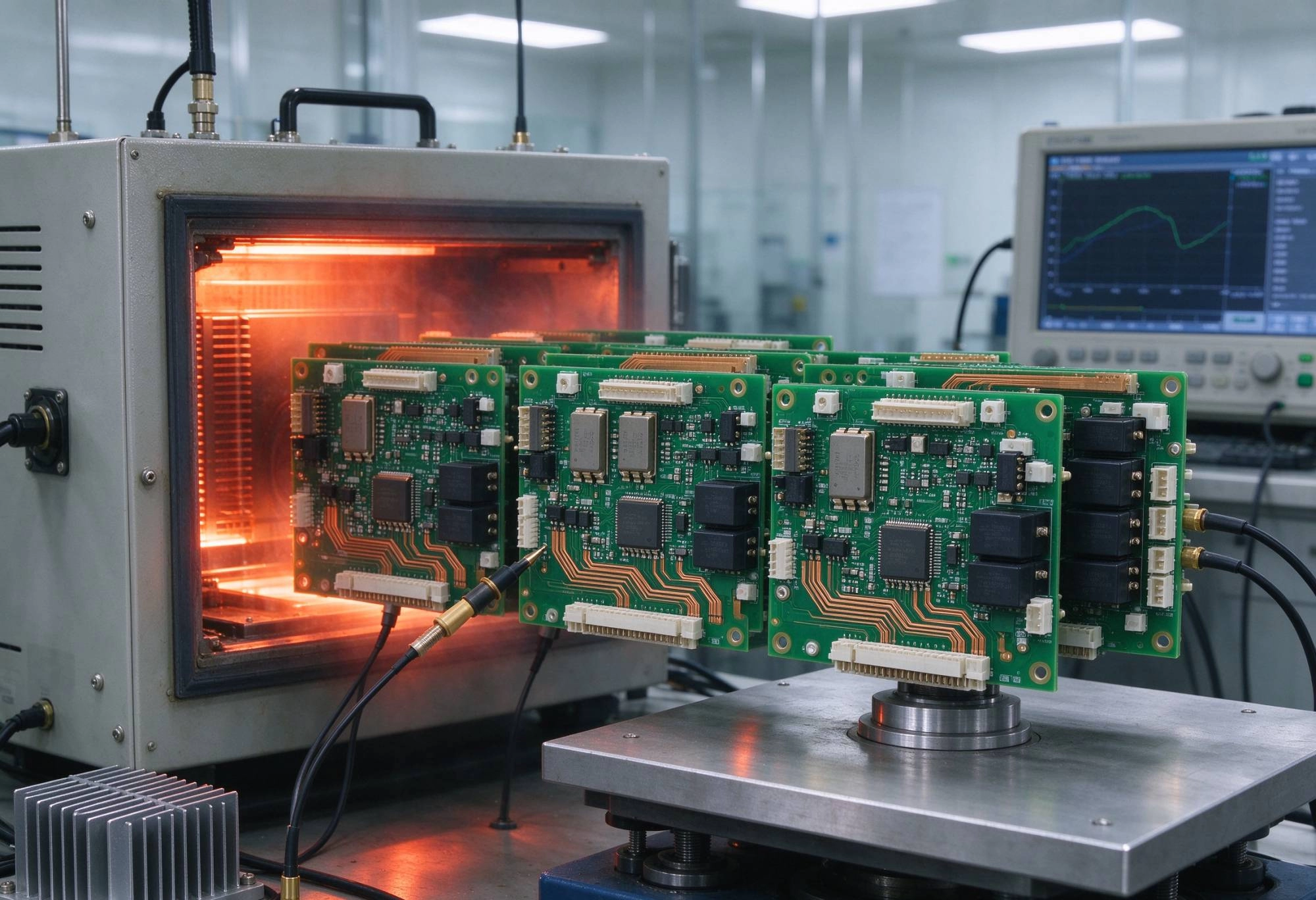
Before releasing an Industrial Pcb design to production, validate it with these tests:

TestStandardPurpose
Thermal cyclingIPC-TM-650 2.6.7500–1000 cycles, -40°C to +85°C; detects solder joint fatigue and via cracking
Thermal shockMIL-STD-202G Method 107Rapid temperature transitions; more aggressive than cycling
Humidity testingIEC 60068-2-7885°C/85% RH for 1000 hours; detects CAF, corrosion, and insulation breakdown
VibrationIEC 60068-2-65–500 Hz sinusoidal vibration; verifies mechanical robustness
ShockIEC 60068-2-27Half-sine shock pulses; simulates drops and impacts
Salt sprayIEC 60068-2-11Corrosion resistance for coastal or chemical environments
Burn-inCustomer-defined48–168 hours at rated load; screens infant mortality failures

Don't skip these tests to save time. A failure caught during qualification costs hundreds of dollars. A failure in the field costs thousands — or millions.

Long-Term Supply Chain Management

A 10-year product needs a 10-year supply chain. Strategies:

  • Avoid end-of-life (EOL) components in new designs; check manufacturer lifecycle status before finalizing BOM
  • Specify second-source components for critical parts
  • Buy lifetime inventory of key components when a manufacturer announces EOL
  • Document all substitutions and validate them with regression testing
  • Maintain a Component Obsolescence monitoring program with regular BOM reviews

Summary Checklist for 10-Year Industrial PCB Design

  • ☐ High-Tg substrate (Tg ≥ 170°C) with appropriate CTE
  • ☐ Adequate copper weight for current carrying and thermal performance
  • ☐ Ipc-6012 Class 3 via plating for thermal cycling reliability
  • ☐ ENIG or ENEPIG surface finish for solderability and shelf life
  • ☐ Component derating: 50–70% voltage, 20°C temperature margin
  • ☐ Thermal Vias and copper pours for Heat Dissipation
  • ☐ Solder joint reinforcement for vibration-prone components
  • ☐ Conformal Coating specified for the operating environment
  • ☐ DFM/Dft features included in layout
  • ☐ Qualification testing completed and documented
  • ☐ Long-term component availability verified
  • ☐ Full documentation package: Gerber, BOM, assembly drawings, test procedures

Designing for 10+ years of operation isn't about using the most expensive materials or the most aggressive testing — it's about disciplined engineering at every step. The boards that survive a decade in the field are the ones where every design decision was made with longevity in mind.
Send Message
Name*
E-mail*
Country*
Phone/WhatsApp*
Name*
E-mail*
Country*
Phone/WhatsApp*