

High-density interconnect boards pack more functionality into smaller spaces than ever before, but miniaturization creates mechanical vulnerability. Tiny vias, thin dielectrics, and fine features that enable dense routing also reduce the structural robustness of the board. As Hdi Technology advances into applications from medical implants to aerospace systems where reliability is critical, understanding how to enhance mechanical strength becomes essential for design engineers.
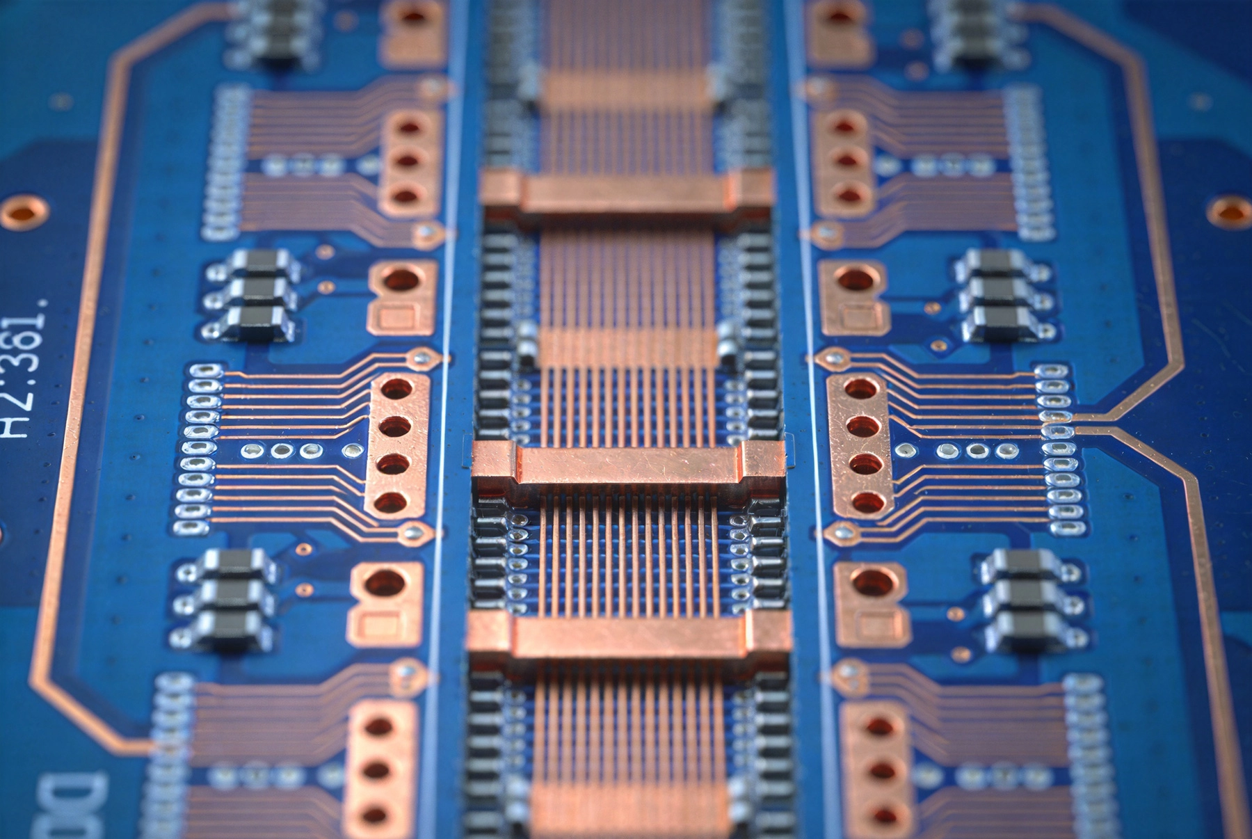
HDI structures differ fundamentally from traditional multilayer boards in their mechanical characteristics. Standard multilayer boards use relatively thick dielectric layers and large through-holes that provide inherent structural rigidity. HDI boards use thin dielectrics, laser-ablated Microvias, and sequential build-up layers that prioritize electrical performance over mechanical robustness.
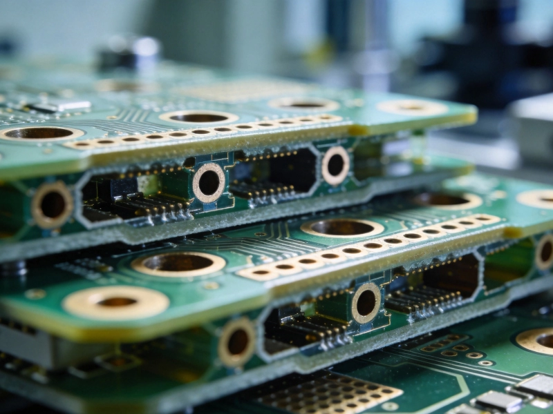
Microvias in HDI constructions are typically 100-300 micrometers in diameter with depths of 50-100 micrometers. The aspect ratios are low, which aids manufacturing but creates stress concentrations at the interface between the via barrel and the pad. When the board experiences Thermal Cycling, these stress points can crack, leading to intermittent opens that are difficult to detect and costly to repair.
The thin dielectric layers between buildup stages range from 40-100 micrometers in thickness. These layers must simultaneously provide electrical insulation, mechanical bonding, and Thermal Management. Balancing these requirements while maintaining adequate strength for the application challenges even experienced HDI designers.
Glass Transition Temperature indicates the temperature at which the substrate transitions from rigid to rubbery state. For HDI applications requiring mechanical strength, selecting materials with elevated Tg values provides better retention of mechanical properties at operating temperatures. Standard FR4 with Tg 130-140C suffices for benign environments, but demanding applications benefit from Tg 170C or higher.
Elastic modulus measures stiffness of the material. Higher modulus substrates resist deflection and bending better than flexible low-modulus materials. When HDI boards must survive mechanical shock or vibration, modulus becomes a critical selection criterion. Some specialty substrates achieve modulus values 50% higher than standard FR4 while maintaining good processability.
Thermal expansion coefficient must be managed carefully in HDI constructions. The CTE mismatch between copper, dielectric, and any surface coatings creates stress during temperature changes. Low-CTE materials reduce this stress and improve joint reliability for surface-mounted components. Ceramic-filled substrates offer lower CTE than glass-reinforced options, though at increased cost.
Standard FR4 uses woven glass fiber reinforcement that provides strength but creates anisotropic behavior where properties differ in weave versus perpendicular directions. Non-woven glass or aramid reinforcement offers more isotropic characteristics that distribute stress more evenly across the board.
For HDI boards requiring maximum strength, hybrid constructions combine different reinforcement types in specific layers. A central core with woven glass provides primary structural support, while buildup layers use more flexible non-woven materials that accommodate the fine feature processing. This approach optimizes both strength and manufacturability.
Metal-core substrates solve thermal and strength challenges simultaneously by incorporating aluminum or copper substrates beneath the HDI layers. These constructions provide excellent heat spreading while the metal core adds rigidity. The thermal expansion of metal cores can be matched to the HDI dielectric to reduce stress at the interface.
Stacked microvia constructions place vias directly atop one another, connecting layer one to layer two, then layer two to layer three. This arrangement enables the highest routing density but creates stress concentrations along the via stack. When thermal stress occurs, cracks typically initiate at the interface between stacked vias.
Staggered via arrangements offset vias from each other so that stress points are distributed across a larger area. A via from layer one to layer two does not sit directly beneath a via from layer two to layer three. This separation reduces the intensity of stress concentration and improves fatigue life during Thermal Cycling.
For applications requiring maximum reliability, staggered designs with generous pad sizes provide the best mechanical performance. The trade-off is reduced routing density, but for applications where reliability outweighs density, this compromise is worthwhile.
Via-in-pad with filled and capped vias eliminates the stress concentration point at the surface pad. The via barrel is filled with resin or conductive paste, then the surface is planarized to create a solid pad without a depression. This structure distributes stress more evenly and prevents solder wicking into the via barrel during assembly.
Conductivepaste filling provides additional reinforcement compared to resin filling alone. The conductive material bonds better to the barrel walls and maintains electrical continuity if minor cracking occurs. Some manufacturers offer proprietary filling compounds specifically designed for mechanical reinforcement.
Back-drilling of through-holes adjacent to microvia stacks removes the stub that would otherwise create impedance discontinuities and mechanical weak points. While technically different from microvia reinforcement, back-drilling contributes to overall structural integrity by eliminating unnecessary copper and dielectric layers from the signal path.
Landing pad dimensions significantly affect HDI reliability. Larger pads provide more area for stress distribution and better thermal conduction away from solder joints. For fine-pitch components like 0.4mm pitch BGAs, pad dimensions are constrained by the component pitch, but within those constraints, maximizing pad size improves reliability.
Non-Solder Mask defined versus Solder Mask defined pads affect mechanical strength differently. NSMD pads where the solder mask is pulled back from the pad create a cleaner solder joint but leave less substrate support around the pad. SMD pads where solder mask covers part of the pad provide more substrate backing but can affect solder joint shape and reliability under thermal stress.
Teardrop attachments that widen the trace approaching a pad reduce stress concentration at this critical junction. The teardrop geometry distributes stress more gradually and prevents crack initiation at the trace-pad interface. Many HDI designers automatically include teardrops on all pad connections without significant routing penalty.
The core substrate beneath HDI buildup layers provides most of the mechanical strength in the board. Using a thicker core increases overall rigidity but adds to total board thickness and weight. For applications with specific thickness constraints, optimizing core thickness for the minimum acceptable strength becomes a design exercise.
Symmetric core construction where buildup layers are balanced on both sides of the core reduces warp tendency. If all buildup occurs on one side, the board may bow as thermal expansion differs between the buildup and core sides. Symmetry ensures that expansion forces cancel out.
For thick cores exceeding 1.5mm, through-hole reliability improves due to increased mechanical support, but drilling and plating costs increase. The optimum core thickness balances manufacturing cost, board flexibility, and hole reliability for the specific application.
Sequential Lamination builds HDI layers in stages rather than pressing all layers simultaneously. Each lamination cycle exposes previously built layers to additional heat and pressure. While sequential building enables complex layer structures, it introduces cumulative stress that can affect reliability.
Reducing the number of lamination cycles improves mechanical outcomes. Design approaches that minimize sequential steps reduce the stress exposure and improve final board integrity. Any-layer HDI constructions that eliminate the need for Sequential Lamination provide the best mechanical properties for the most complex designs.
Annealing steps between sequential laminations can relieve internal stress and improve mechanical stability. Some manufacturers incorporate controlled cooling cycles and stress relief steps in their sequential build processes. Ask about process steps when evaluating HDI capabilities.
The weakest link in most HDI assemblies is the solder joint between the component and the board. Fine-pitch components with small pads create inherently fragile joints that thermal cycling and mechanical shock can fail. Enhancing HDI mechanical strength means ensuring these joints survive expected stress conditions.
Underfill materials that fill the gap beneath area array packages like BGAs significantly improve joint reliability. The underfill adhesive transfers stress from the package to the board over a larger area, reducing stress concentration at individual joints. For ceramic BGAs with high CTE mismatch to organic boards, underfill is often mandatory for field reliability.
Glob-top coating and potting of sensitive areas provides additional protection against mechanical shock and vibration. These materials encapsulate components and prevent movement that could crack joints. The trade-off is reduced repairability and potential thermal issues if the coating traps heat.
Thermal cycling causes differential expansion between components, solder joints, and board substrate. Each material has its own CTE, and the differences create stress at interfaces. The number of cycles, temperature range, and rate of change all affect fatigue accumulation in solder joints.
Lead-free solders like SAC305 have higher elastic modulus than traditional tin-lead and experience greater stress under thermal cycling. This makes mechanical optimization of HDI structures even more important when using lead-free assembly processes required by environmental regulations.
Accelerated Life Testing that simulates field thermal cycling conditions verifies that HDI designs meet reliability targets. Standard tests like IPC-9701 define test conditions and acceptance criteria for surface mount attachments. Include appropriate testing in your qualification plan for demanding applications.
Copper plating uniformity in microvia barrels directly affects mechanical strength. Thin plating creates weak points that crack under stress, while uniform plating distributes stress more evenly. The Plating Process parameters including current density, solution chemistry, and agitation affect the quality of deposited copper.
Electroless nickel palladium gold finishing provides excellent surface flatness and solderability but adds multiple material layers with different mechanical properties. The total stack-up of finish layers affects stress distribution at pad surfaces. Evaluate finish options not just for solderability but also for mechanical compatibility with your stress conditions.
Void-free plating that avoids trapped bubbles or inclusions in via barrels improves mechanical properties. Voids create stress concentrations that can initiate cracking. Ask manufacturers about their Plating Process controls and void inspection methods for critical applications.
Lamination process parameters set the mechanical properties of the finished board. Insufficient pressure leaves weak bonds between layers, while excessive pressure can squeeze resin away from critical areas or deform fine features. Temperature profile affects how well resin flows and fills gaps before curing.
Vacuum lamination that removes air before and during pressing reduces void formation and improves layer-to-layer bonding. Many HDI manufacturers use vacuum-assisted lamination as standard practice due to the improved bond quality it provides.
Post-lamination annealing relieves internal stresses and stabilizes the board dimensions. This additional process step improves mechanical stability and reduces the tendency for boards to warp over time. For demanding applications, specify post-lamination stress relief as part of your manufacturing requirements.
Cross-sectioning boards to examine via structure and plating quality provides direct evidence of mechanical integrity. This destructive test reveals internal defects that noinspection (inspection) method can detect. Standard IPC acceptance criteria define minimum plating thickness and acceptable defect types.
Pull testing of through-holes and microvias measures the force required to separate the barrel from the pad. Higher pull strength indicates better mechanical bonding. Typical minimum pull strengths are specified in manufacturing standards, but demanding applications may require higher values.
Shear testing measures component attachment strength by applying lateral force to components on the board. This test reveals whether component pads, substrate, and solder joints can withstand expected shear stresses from thermal mismatch or mechanical shock.
Acoustic micro-imaging uses ultrasonic waves to detect delaminations, voids, and cracks without damaging the board. This technique examines internal structure through water immersion scanning. Any-planar (any-layer) HDI boards benefit from acoustic inspection at multiple stages of production.
X-ray Inspection reveals internal structure including plating quality and void content. While standard X-ray provides 2D projection images, CT scanning offers 3D volumetric analysis. For critical applications, CT inspection of sample units provides the most complete characterization of internal structure.
Thermal cycling with intermittent continuity monitoring detects opens that occur only when the board is heated or cooled. Boards that pass room-temperature testing may fail during thermal stress. Continuous monitoring during cycling identifies failures that would otherwise be missed.
Designing for mechanical strength begins with setting appropriate design rules for your reliability requirements. Higher reliability applications warrant more conservative design rules including larger pads, wider spacing, and more robust via structures. Early design decisions lock in the achievable strength of the finished board.
Minimize the number of sequential build-up layers to reduce cumulative lamination stress. Where possible, use any-layer constructions that eliminate sequential requirements. If sequential building is necessary, minimize the number of build stages.
Include design-for-test features that enable verification of mechanical integrity. Test coupons that represent the actual board construction provide correlation between qualification testing and production boards. These coupons can be destructively tested without sacrificing functional boards.
Document your mechanical requirements clearly when communicating with manufacturers. Explicit specifications for plating thickness, pull strength, and other mechanical parameters enable appropriate process controls and inspection.
Automotive Electronics must survive temperature cycling from -40C to +150C or higher, vibration, and humidity without failure. The AEC-Q100 and AEC-Q200 qualification standards define mechanical and environmental test requirements. HDI designs for automotive must meet these demanding test conditions.
Automotive manufacturers typically require PPAP documentation including process capability indices for critical parameters. Designing boards that achieve Cpk values above 1.33 for hole plating and other mechanical parameters demonstrates statistical process control adequate for automotive quality systems.
Implantable medical devices using HDI must remain functional for decades inside the human body. The mechanical environment includes body temperature constant at 37C but also tissue pressure and movement. HDI for medical implants requires special materials compatible with body chemistry and sterilization processes.
Non-implantable medical devices still face stringent reliability requirements. Many medical electronic systems must function for the lifetime of the device, often ten years or more. HDI designs for medical applications require thorough qualification testing including accelerated aging and environmental exposure.
Military and aerospace applications expose HDI boards to extreme temperature ranges, high altitude pressure, and vibration from engines and aerodynamic loads. The defense industry has developed specialized HDI requirements in standards like MIL-PRF-31032 and MIL-PRF-55110 that specify mechanical and environmental performance.
Bond strength requirements for aerospace HDI typically exceed commercial standards. Peel strength, pull strength, and other mechanical tests define minimum acceptable values that ensure survival in demanding flight environments.
Enhancing mechanical strength of HDI structures requires attention to Material Selection, via design, layer buildup strategy, and manufacturing process controls. Each decision from substrate choice through final inspection affects the mechanical robustness of the finished board.
Material Selection should prioritize high Tg and high modulus substrates when strength is critical. Reinforced laminates and metal-core constructions provide additional rigidity for demanding applications. The substrate beneath buildup layers carries most of the mechanical load.
Via design optimization using staggered arrangements, reinforced pad structures, and proper plating quality reduces stress concentrations that cause cracking. Teardrop attachments and Via-in-pad constructions distribute stress more evenly across critical junctions.
Manufacturing process controls including vacuum lamination, proper plating parameters, and post-lamination stress relief improve mechanical properties. These process decisions must be communicated to manufacturers as explicit requirements.
Testing and verification through destructive analysis and non-destructive inspection confirms that designs achieve intended strength targets. Qualification testing that simulates field conditions validates reliability for the specific application environment.
By considering mechanical strength from the earliest design stages and maintaining appropriate requirements throughout development, HDI boards can meet the reliability expectations of demanding applications while delivering the electrical performance that makes Hdi Technology valuable.
Ensuring Industrial PCB Reliability in Extreme Environmental ConditionsMay/27/2026
How to Prevent Electrochemical Migration (CAF) for Better Industrial PCB ReliabilitySeptember/04/2026
The Role of Conformal Coating in Enhancing Industrial PCB ReliabilityJuly/17/2026
Managing Moisture Sensitivity Levels (MSL) in Industrial PCBAOctober/22/2026
Vibration and Shock: Designing for Industrial PCB Reliability in AutomationJune/30/2026
Thermal Management Strategies for Long-Term Industrial PCB ReliabilityJune/04/2026
Top 5 Causes of Failure and How to Improve Industrial PCB ReliabilitySeptember/21/2026
Via-in-Pad and Microvias: Key Features of Advanced HDI SolutionsJuly/26/2026