Open Nav


You have spent weeks on your Industrial Pcb design. The schematic is clean, the layout is routed, and simulation says it will work. But will it fabricate correctly? Will it assemble without defects? Will it survive the Thermal Cycling and vibration of an industrial environment for years?
The gap between "the design works in CAD" and "the board can be reliably manufactured and assembled" is where DFM—Design For Manufacturing—lives. And it is a gap that swallows projects whole. Every year, engineers lose weeks to redesigns forced by fabrication failures: traces too fine to etch, pads too small for drill registration, Solder Mask slivers that flake off, and stackups that warp like potato chips in the reflow oven.
This checklist is your pre-tape-out safety net. Work through it methodically before you generate your final Gerber files. Every check that fails is a potential fabrication or assembly defect—and a delay you can avoid.

The stackup is the foundation of your board. Get it wrong and everything built on top—impedance, Thermal Management, warpage control—is compromised.
Your fabrication drawing must specify every layer's material, thickness, and copper weight. Do not leave any layer undefined. The fabricator will make assumptions, and their assumptions may not match your impedance or thermal requirements.
Asymmetrical stackups—different copper distribution or laminate thicknesses on opposite sides of the core—cause warpage after lamination and reflow. Warped boards do not sit flat on pick-and-place machines, cause BGA opens during reflow, and do not make proper contact with heatsinks. Mirror the copper and dielectric distribution about the board centerline.
Standard FR-4 core thicknesses are 0.005", 0.008", 0.014", 0.021", 0.028", 0.036", 0.047", 0.059", and 0.093". Non-standard thicknesses require custom orders from the laminate manufacturer, adding cost and lead time. Build your stackup from standard values.
Verify that trace widths at the specified copper weight can carry the required current per IPC-2152. For power traces carrying more than 2-3A, 2 oz copper is typically the minimum. For very high currents (above 10A), consider 3 oz or heavier, or copper pours with via stitching. Remember that internal layers carry less current than external layers of the same width and copper weight because they cannot convect heat to air.
Standard FR-4 (Tg 130-140°C) is adequate for many industrial applications. If your board will experience high operating temperatures (above 105°C ambient), frequent Thermal Cycling, or lead-free reflow on a thick board, specify High-tg Fr-4 (Tg 170°C or above). For extreme environments, polyimide or ceramic-filled laminates may be required.
Trace and space violations are the most common reason for fabrication quotes to come back with caveats—or for fabricated boards to fail.
Check the fabricator's capability list for their minimum trace/space at the copper weight you have specified. Typical values are 4/4 mil for 1 oz copper and 5/5 mil or 6/6 mil for 2 oz copper. If you have traces below the minimum, widen them or change the routing layer.
Do not use IPC-2221 (the older standard) for current-carrying capacity calculations—it is conservative but outdated. IPC-2152 provides more accurate capacity data that accounts for the actual board configuration. For industrial Power Electronics, undersized traces are a fire risk.
Acute angles cause etching problems—the etchant undercuts the narrow point, creating a neck-down that increases resistance and may fail under current. Most CAD tools flag acute angles automatically, but review any that remain.
Traces that neck down to route between pads—common on BGA fanouts—must maintain adequate width for their current. A 12 mil power trace that necks to 4 mil between BGA pads may not carry the required current even if the 4 mil width meets the fabricator's minimum trace rule.
For Differential Pairs, verify that the pair-to-pair spacing and intra-pair spacing are consistent throughout the route, and that the pair lengths are matched within the required tolerance (typically 5 mil for high-speed signals). Check that the pairs are not routed over splits in reference planes, which destroys the return path and degrades Signal Integrity.
Pads and vias are the interface between your design and the physical board—and the source of many assembly defects.
This is the most important check in the entire list. Compare every footprint against the component manufacturer's recommended land pattern. Pay special attention to:
One wrong footprint can make every board in the build non-functional.
The annular ring—the copper pad area remaining after the drill hole—is your margin against drill registration error. For standard through-holes, the minimum annular ring should be at least 5 mil (0.127mm) on inner layers and 4 mil on outer layers for Class 2 boards. For Class 3 (aerospace, medical), increase these to 7 mil and 5 mil respectively. If your fabricator's drill registration capability is ±3 mil, a 5 mil annular ring leaves only 2 mil of pad after worst-case misregistration—tight but acceptable.
Aspect ratio (board thickness ÷ drill diameter) is a key plating reliability parameter. For standard through-hole plating, keep aspect ratios at or below 6:1 for reliable plating. High aspect ratios (8:1 and above) require special plating processes and have lower yield. For very thick boards, consider using Hdi Technology with Microvias instead of high-aspect-ratio through-holes.
Pads connected to power or ground planes without thermal relief spokes are difficult to solder—the plane acts as a massive heat sink that prevents the pad from reaching soldering temperature. For through-hole pads on planes, four thermal relief spokes (typical width 8-12 mil, connecting to a 20-40 mil diameter pad) are standard. SMT pads on planes should also have thermal reliefs if hand soldering or rework is anticipated.
Mounting holes and tooling holes that should not be plated must be defined as non-plated in the drill file. If a mounting hole is accidentally plated, it creates an electrical connection to internal planes (if the hole intersects them) and prevents proper screw mounting. Verify that non-plated holes have no connection to any net.
Unplated vias in BGA pads can wick solder away from the joint during reflow (solder thieving), creating weak joints. Define whether vias should be tented (covered with Solder Mask), plugged (filled with epoxy and capped with copper), or left open. For Via-in-pad designs, plugged vias are essential—do not leave this decision to the fabricator.
Solder mask openings are typically 2-4 mil larger than the copper pad on each side (solder mask expansion). For fine-pitch components, excessive expansion can create solder mask slivers—narrow strips of mask between adjacent pads that may not adhere reliably. If slivers are below 4 mil wide, reduce the expansion or merge adjacent openings.
Solder mask on a solderable pad prevents proper wetting. Run a DFM check specifically for solder mask-to-pad violations. This is especially important for QFN thermal pads, which are sometimes partially covered by misaligned solder mask.
Silkscreen ink on a pad interferes with solder joint formation. Most CAD tools check this, but verify—especially for reference designators on small components where the text may encroach on the pads.
Minimum legible text is approximately 0.8mm height with 0.15mm stroke width. Text below this size may print but will be unreadable. If you need small text for space reasons, consider eliminating non-essential Silkscreen markings or using a legend table on the board edge.
Every polarized component—diodes, electrolytic capacitors, ICs—must have an unambiguous indicator. Missing polarity marks cause assembly errors that are difficult to detect visually.
For industrial PCBs that operate at elevated voltages, clearance and creepage distances are safety-critical.
For any net pair with a voltage difference, verify that the shortest air-gap distance between the conductors meets the IEC 60664-1 clearance requirement for the applicable overvoltage category, pollution degree, and altitude. For industrial applications (pollution degree 2, overvoltage category III), common clearance requirements are 0.5mm for 50V, 1.5mm for 150V, 3.0mm for 300V, and 5.5mm for 600V.
For DC voltages, creepage distances along the board surface are typically larger than for equivalent AC voltages because constant electrical stress accelerates surface tracking. Check creepage along all possible surface paths between conductors at different potentials, including around via barrels and along board edges.
Organize the layout so high-voltage and low-voltage sections are in distinct board areas, separated by guard traces at earth potential. This reduces the risk of voltage stress on components not rated for high voltage and minimizes the board area requiring large creepage distances.
Use a field-solver (not a simple Microstrip calculator) to calculate trace widths for your specific stackup. The calculation must account for the actual Dielectric Constant, copper thickness (including plating), trace profile (trapezoidal from etching), and reference plane configuration. Verify that the calculated width is within the fabricator's etching capability.
Test coupons—small sections of board with representative impedance traces—allow TDR measurement during fabrication without probing the actual board. Without coupons, impedance verification requires destructive cross-section or measurement on the board itself, which may not be possible after assembly.
Signals above 100 MHz should have an unbroken reference plane on the immediately adjacent layer. Splits in the reference plane under a high-speed trace cause impedance discontinuities, return path detours, and EMI. Route high-speed signals only over solid plane areas.
For parallel buses and high-speed serial links (DDR, PCIe, USB), verify that length-matched signals are within the required skew tolerance. Account for via length differences—signals that transition between layers through vias of different depths have effective length differences that the CAD length-matching does not capture.
Industrial environments often have high ambient temperatures and limited cooling, making Thermal Management critical.
For every component that dissipates more than 0.5W, verify that there is a low-impedance thermal path from the component to a heatsink, thermal plane, or the board surface. This may involve Thermal Vias under the component, copper pours on the component layer, or connection to internal copper planes through via arrays.
Thermal Vias should have 0.3-0.5mm diameter, 1-2mm spacing, and adequate plating thickness. Verify that the via array does not violate the fabricator's minimum annular ring or create a mechanically weak "Swiss cheese" zone. For Via-in-pad applications, specify copper-filled or epoxy-filled and copper-capped vias.
Are multiple power components clustered in one area? If so, their combined heat output may exceed the board's local heat spreading capacity. Consider spreading hot components apart or adding thermal relief areas (copper pours, additional board layers for heat spreading) in high-dissipation zones.
The PCB does not exist in isolation—it operates inside an enclosure with limited airflow. Verify that the total board power dissipation, combined with the enclosure's thermal resistance, does not result in component junction temperatures exceeding their ratings. If natural convection is insufficient, forced air or heatsinking may be required.
The board outline must be a closed contour in the outline layer, with all internal cutouts defined. Verify that no copper, pads, or components extend beyond the outline. Check that the outline dimensions match the mechanical enclosure requirements.
For prototype quantities, the fabricator typically handles panelization. For production, you may want to specify the panel array, fiducial placement, and tooling hole locations to optimize assembly efficiency. If you specify panelization, ensure fiducials (minimum three, placed in an L-shape pattern) are included on the panel border.
SMT pick-and-place machines require fiducial marks—typically 1-2mm round copper pads with solder mask openings—to align the board in the placement coordinate system. Include at least three global fiducials on the board, plus local fiducials for fine-pitch QFP and BGA components (two per component, diagonally opposed).
Tooling holes (also called mounting holes or registration holes)—typically 3-4mm non-plated holes in the board corners—align the board in assembly fixtures, test fixtures, and wave solder pallets. Place at least two tooling holes on opposite corners, outside the board's component area.
Thin boards (below 0.8mm) may flex during handling, causing misalignment in pick-and-place machines or stress on BGA solder joints. If the board must be thin for application reasons, consider panelization with rigidizing rails, or specify a thicker board if the application allows.
Incomplete documentation forces the fabricator to make assumptions—and their assumptions will favor manufacturability over performance.
Verify that Gerber files use the format expected by the fabricator—typically RS-274X format with 3:3 or 3:4 integer:decimal places, in millimeters or inches (be consistent). Include all copper layers, solder mask layers, silkscreen layers, drill files, and the board outline.
Excellon drill files can use different formats (incremental vs. absolute coordinates, different unit systems, different zero suppression). Mismatches cause the drill machine to drill in the wrong locations. Verify the drill file format against the fabricator's specification, or embed format headers in the file.
Providing the IPC-D-356A netlist allows the fabricator to verify that the electrical test matches your design connectivity. Without it, the fabricator generates their own netlist from the Gerber data—which may not capture your design intent correctly, especially for split planes and complex connectivity.
The fabrication drawing (also called the fab print or board drawing) should include:
If the fabricator is also assembling the board, provide:
Industrial PCBs must survive harsh environments—thermal cycling, vibration, humidity, and sometimes chemical exposure—that consumer boards never face.
Decoupling effectiveness depends on the loop inductance between the IC and the capacitor. Every millimeter of trace length adds inductance that reduces the capacitor's ability to supply transient current. Place bulk decoupling (10-100 µF) within 25mm and local decoupling (0.01-0.1 µF) within 5mm of the IC power pins.
Industrial environments can see temperature swings of -40°C to +85°C or more. This thermal cycling causes differential expansion between components and the board, fatiguing solder joints over time. For components most susceptible to Thermal Fatigue (large BGAs, components with CTE mismatch), consider using corner-staked or underfilled components to reinforce the solder joints.
If the board will be conformal coated, ensure that connectors, Test Points, and any adjustable components are masked or excluded from the coating area. Include keep-out areas for coating on the assembly drawing. Verify that the selected coating is compatible with the board's surface finish and solder mask.
For boards that will experience vibration (industrial machinery, transportation, aerospace), large or heavy components—transformers, large electrolytic capacitors, heavy inductors—require mechanical securing beyond solder joints. This may include adhesive staking, cable ties, or mechanical brackets. Include staking requirements on the assembly drawing.
Conductive Anodic Filament (CAF) growth—copper migration along glass fiber bundles under DC bias and humidity—is a long-term failure mechanism in industrial environments. If the board operates at elevated DC voltage in humid conditions, specify CAF-resistant laminate grades and ensure adequate spacing between biased conductors on inner layers.
A checklist is only useful if you actually use it. Here is a recommended workflow:
Sending a design to fabrication without a thorough DFM review is gambling with your project timeline and budget. The fabrication and assembly process has physical limits and process tolerances that your CAD tool does not inherently respect. The checks in this list—covering stackup, traces, pads, solder mask, clearances, impedance, thermal management, documentation, and reliability—represent the accumulated lessons of countless engineers who learned these lessons the hard way.
No checklist can guarantee zero fabrication problems, but this one dramatically reduces the probability. And the time you spend on DFM before tape-out pays for itself many times over in avoided redesigns, reduced scrap, and faster time-to-working-hardware.
Make this checklist part of your design release process. Customize it for your organization's specific requirements and your fabricator's capabilities. And use it every time—because the one check you skip is the one that will bite you.

Design for Testability (DFT): A Crucial Aspect of Industrial PCB DesignJuly/20/2026
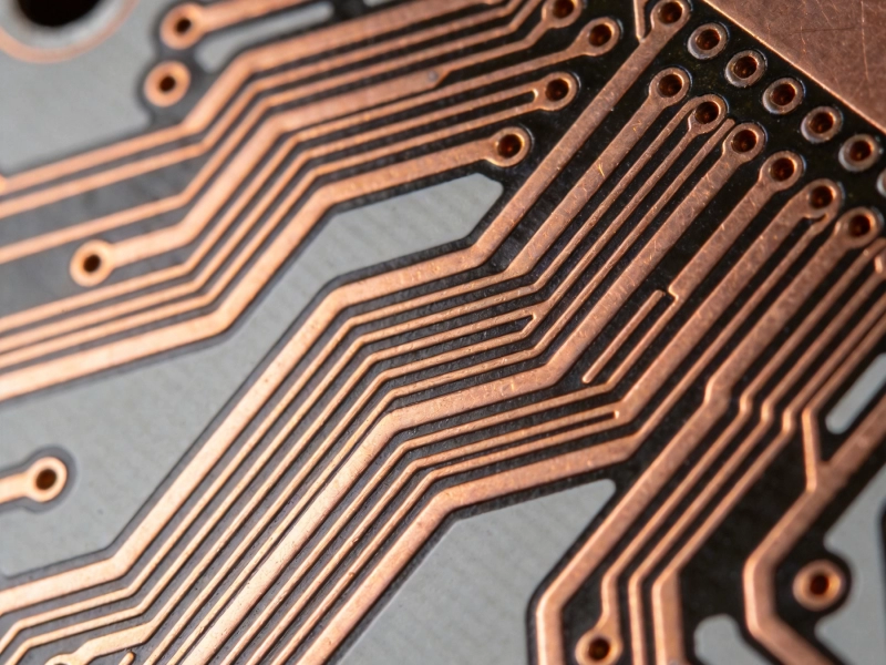
Optimizing Trace Width and Spacing in Industrial PCB DFMAugust/06/2026
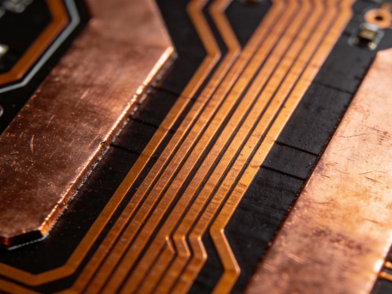
Design Rules for Heavy Copper Traces in Power ElectronicsJuly/27/2026

Panelization Strategies for Efficient Industrial PCB Design and AssemblySeptember/08/2026

Essential Rules for Industrial PCB DesignJune/08/2026
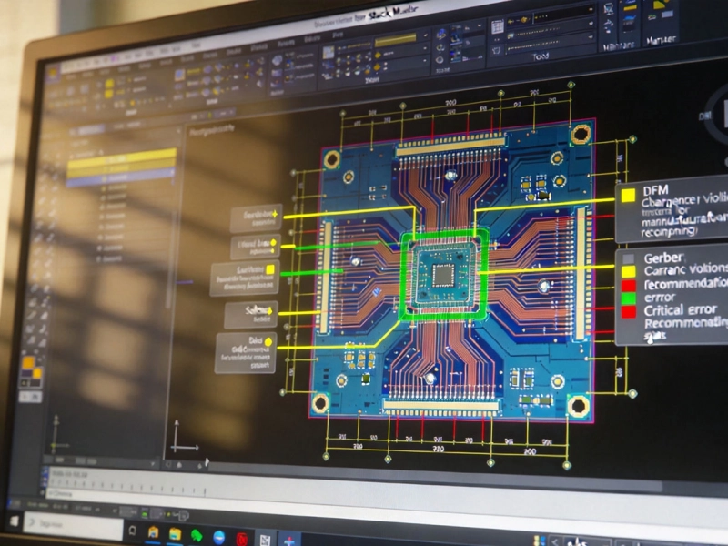
Essential Rules for Industrial PCB DesignMay/27/2026
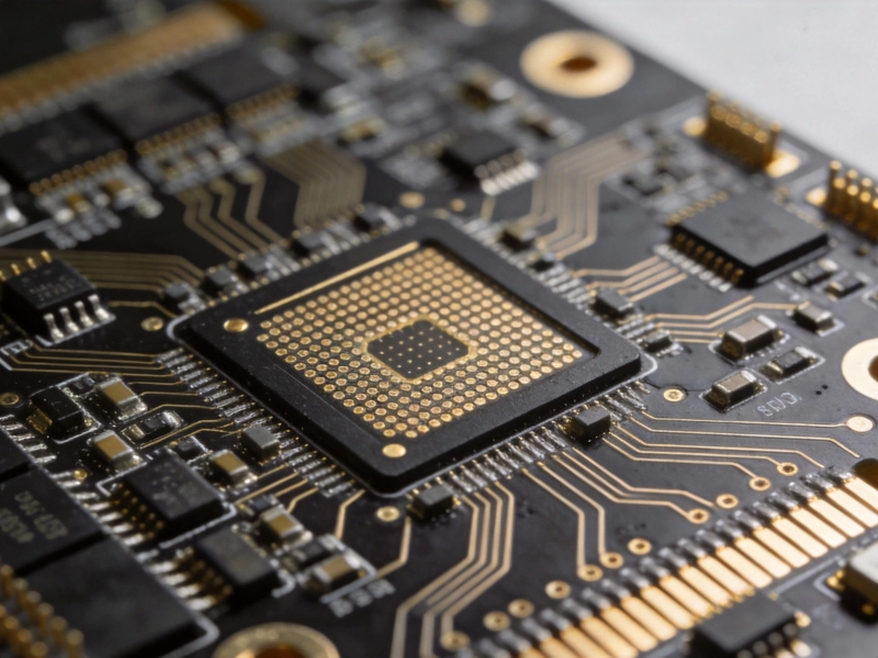
Cost vs. Performance: When to Use HDI Solutions in Industrial DesignSeptember/14/2026
How to Avoid Costly Mistakes with Proper Industrial PCB DFMJuly/03/2026