Open Nav


High Density Interconnect (HDI) PCBs deliver superior routing density, smaller via structures, and better electrical performance than conventional multilayer boards. These advantages come at a price—HDI boards cost more to fabricate and require more precise process control. The question for industrial designers is not whether HDI is better, but whether the performance benefits justify the cost premium for your specific application.
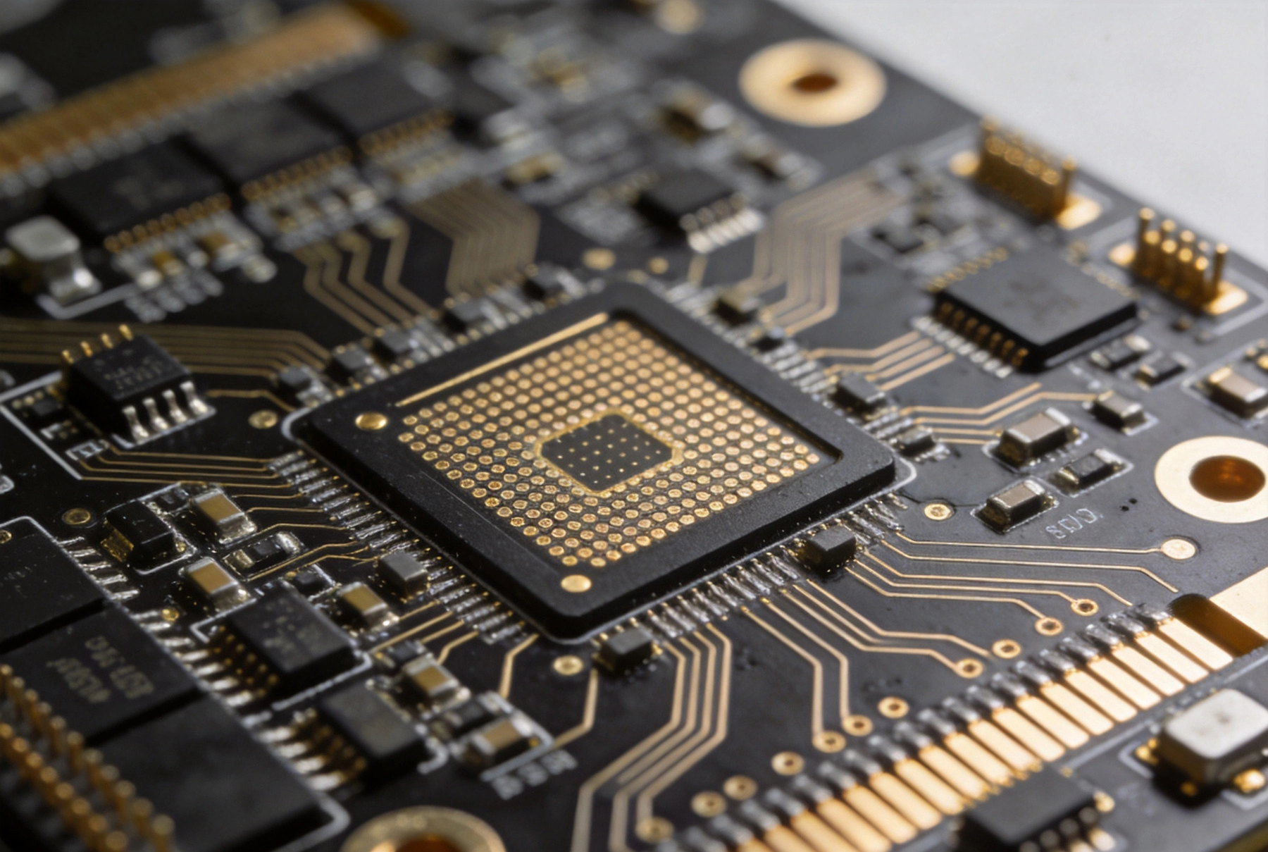
HDI encompasses a set of fabrication techniques that achieve higher interconnect density than standard multilayer processes. The core differentiators are Microvias—holes typically 0.15 mm or smaller in diameter—and Sequential Lamination, which allows blind and buried vias to connect specific layers without consuming routing space on outer layers.
Standard through-hole vias pass through every layer of a board, consuming routing channels from the top layer to the bottom even when a connection is only needed between two adjacent layers. HDI's blind and buried vias connect only the layers they need to, freeing up routing space and enabling finer trace and space geometries.
The result is a board that can accommodate more traces in the same area, support finer pitch components, and reduce the overall board size needed to implement a given circuit. For products where miniaturization matters, HDI is often the only viable path forward.
HDI is justified when your design cannot meet its requirements using standard multilayer fabrication. This happens in several common scenarios.
Fine pitch components like 0.3 mm pitch BGAs require microvia fanout that standard through-hole technology cannot achieve reliably. A 0.3 mm pitch BGA has pads spaced 0.3 mm apart—too close for standard drill and plating processes to create reliable vias in the escape pattern. HDI Microvias with their smaller diameters and precise registration can fan out from these tight pad patterns to inner layer routing.
High-speed Signal Integrity benefits from HDI's reduced via stub length. Through-hole vias act as stubs that create resonances at certain frequencies, degrading signal quality. Blind Vias connect only the layers needed for the signal path, eliminating the stub and extending the usable frequency range.
High-layer-count designs that need to stay within a reasonable board outline benefit from HDI's routing efficiency. A 12-layer board designed with Hdi Technology can often achieve the same routing capacity as a 16-layer or even 20-layer board using conventional processes, at lower cost and with better electrical performance.
Products with aggressive miniaturization targets benefit from HDI's ability to pack more function into less area. If your product must fit a small enclosure and contains many components, HDI lets you use smaller board dimensions or accommodate more features in the same footprint.
HDI fabrication is inherently more expensive than standard multilayer production. The cost drivers are numerous and additive.
Material costs are higher because HDI boards typically require laser drills, Sequential Lamination cycles, and thin dielectric cores that are more expensive than standard prepreg. The lamination press cycles are longer and require more precise temperature and pressure control.
Process complexity drives yield losses. Each additional lamination cycle introduces potential for Delamination, voiding, or registration error. The tighter tolerances of HDI mean that process variations that would be acceptable in standard boards cause failures in HDI. These yield losses translate directly into higher unit costs.
Testing is more involved. Microvias require electrical test coverage that can detect opens or high-resistance connections in small via structures. Standard flying probe or fixture-based test may not provide adequate coverage for microvia chains, requiring additional test approaches.
A typical HDI board costs 1.5 to 3 times more per square inch than an equivalent standard multilayer. The premium varies with layer count, via density, and the specific HDI structure type—Type I HDI (Blind Vias on one side only) is less expensive than Type III (blind and buried vias on multiple layer pairs). For high-volume products where the board cost is a small fraction of total product cost, this premium may be acceptable. For cost-sensitive products, it can make HDI impractical.
Before defaulting to HDI, explore whether a well-designed standard multilayer board can meet your needs. Careful layout optimization—using inner layer ground planes for shielding, optimizing trace routing to minimize layer count, and selecting components with more manageable pitch—can stretch the capabilities of conventional processes.
For many industrial control applications, a well-designed 6-layer or 8-layer board with standard through-hole technology provides adequate routing and Signal Integrity. These designs are less expensive, have higher fabrication yields, and can be produced by a wider range of manufacturers.
Consider also whether a hybrid approach makes sense. Use standard multilayer for most of the board and reserve HDI only for the section with the densest components or most demanding signal requirements. Some manufacturers support this mixed-technology approach, though it requires careful process planning.
The IPC-2315 standard defines HDI structure types that range from simple to complex. Understanding these types helps you specify the right level of HDI complexity for your design.
Type I HDI adds a single buildup layer over a standard core, with laser-drilled blind vias connecting the buildup layer to the core. This is the least complex HDI option and is appropriate for designs with moderate density requirements, such as boards with 0.4 mm pitch BGAs that need microvia fanout but do not require complex routing.
Type II HDI adds buildup layers on both sides of the core, with blind vias on both surfaces. This enables higher routing density and supports designs with components on both sides of the board that require microvia fanout. Type II is common in smartphone and tablet applications and is increasingly used in industrial IoT devices.
Type III HDI adds multiple buildup layers on one or both sides of the core, with buried vias connecting internal layer pairs in addition to blind vias on the surfaces. This is the most complex HDI type and is used for the highest-density designs, such as advanced processors with 0.25 mm or finer pitch BGAs and demanding routing requirements.
Any-layer HDI, sometimes called "any-layer interconnect" or ALIVH, uses laser vias throughout the stack-up with all layers available for any-to-any connectivity. This provides maximum routing flexibility and is used for the most advanced applications where density requirements exceed what even Type III can provide.
The decision framework starts with your component selection. If your design uses fine-pitch BGAs at 0.4 mm pitch or finer, HDI microvia fanout is almost certainly necessary for reliable assembly. If your finest pitch is 0.5 mm or larger, standard multilayer may handle the escape routing depending on the BGA pin count and your routing density requirements.
Signal speed is another factor. For digital signals at 5 Gbps or higher, or for RF applications above a few GHz, HDI's reduced via stub length and better impedance control provide measurable signal integrity benefits. For lower-speed signals, the electrical advantage of HDI may not be relevant to your application.
Board size constraints drive the decision when you need more features than a conventional board of the available size can provide. If you are designing to a fixed board outline and your routing does not fit, HDI lets you pack more traces into the same area. If you can specify a larger board outline, you may achieve the same result with standard multilayer at lower cost.
HDI fabrication requires specialized capabilities that not all manufacturers possess. Before committing to HDI, verify that your chosen fabricator has the equipment, process controls, and quality systems to produce your design reliably.
Ask about their HDI experience—the types of structures they have produced, their minimum microvia size, their registration tolerances, and their typical yields for HDI work. Request a design review from their engineering team, as they can identify potential manufacturability issues before you commit to production.
Be prepared for longer lead times on HDI boards. The sequential lamination process takes more time than standard multilayer lamination, and the tighter process controls mean more frequent in-process inspection. Typical HDI lead times run 2–3 weeks longer than standard multilayer, though this varies by manufacturer.
HDI is a powerful technology that enables designs that would be impossible with conventional processes. But it is not always the right choice. Weigh the performance benefits against the cost and complexity premium, and reserve HDI for applications where its capabilities are truly needed. For everything else, a well-optimized standard multilayer board delivers reliable performance at a lower price point.
Essential Rules for Industrial PCB DesignJune/08/2026

Panelization Strategies for Efficient Industrial PCB Design and AssemblySeptember/08/2026
Design Rules for Heavy Copper Traces in Power ElectronicsJuly/27/2026
How to Avoid Costly Mistakes with Proper Industrial PCB DFMJuly/03/2026
Essential Rules for Industrial PCB DesignMay/27/2026
Optimizing Trace Width and Spacing in Industrial PCB DFMAugust/06/2026
Design for Testability (DFT): A Crucial Aspect of Industrial PCB DesignJuly/20/2026
Material Selection Guide for High-Speed Industrial PCB SolutionsJuly/14/2026