Open Nav


Thermal Management is one of the most critical design challenges in modern electronics. As power densities increase in LED lighting, automotive electronics, power supplies, and RF amplifiers, traditional FR-4 substrates reach their thermal limits. Metal Core PCBs (MCPCBs)—also known as Insulated Metal Substrate (IMS) boards—have emerged as the go-to solution for high-power applications. However, the performance of an Mcpcb hinges on two interrelated factors: the thermal resistance of the dielectric layer and the material properties of the dielectric itself. This article explores how these elements work together, how to evaluate them, and how to make informed design choices for your Metal Core Pcb projects.
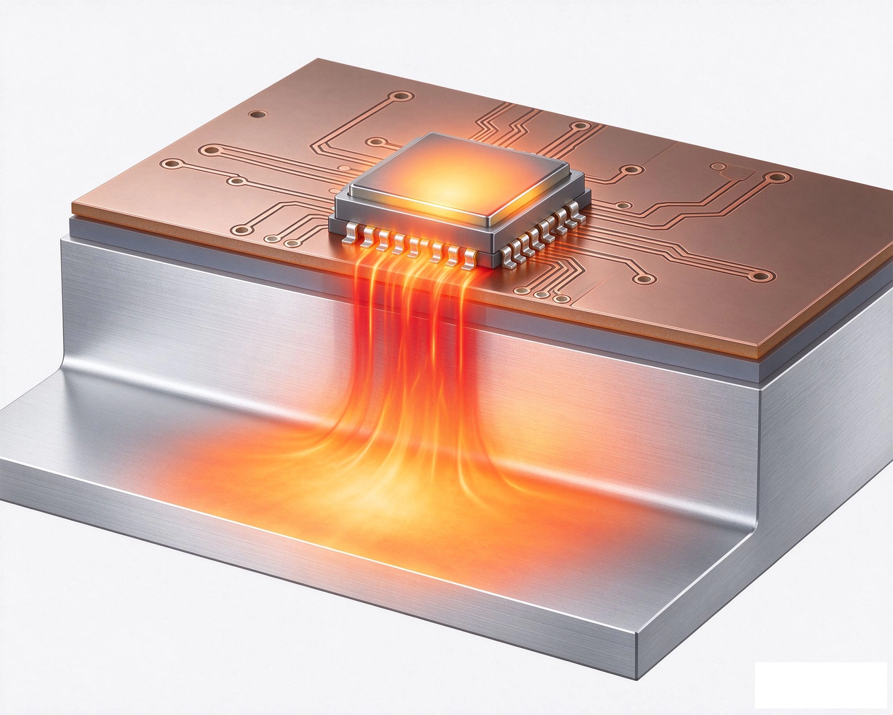
A Metal Core Pcb is a type of printed circuit board that uses a metal substrate—typically aluminum, copper, or a copper-aluminum alloy—as its base layer instead of the traditional fiberglass-reinforced epoxy (FR-4). The metal core acts as a heat spreader, conducting thermal energy away from heat-generating components and dissipating it through the board structure or into an external heatsink.
A typical Mcpcb consists of three layers:
The dielectric layer is the linchpin of this structure. It must simultaneously provide electrical isolation between the circuit and the metal core while enabling efficient heat transfer—a seemingly contradictory requirement that drives material innovation in the MCPCB industry.
Thermal resistance, denoted as Rth or θ, is the measure of a material's opposition to heat flow. In the context of MCPCBs, it quantifies how effectively heat can travel from the component junction through the dielectric layer and into the metal core. Lower thermal resistance means better Heat Dissipation.
The thermal resistance of a planar layer is calculated as:
Rth = t / (k × A)
Where:
For MCPCB designers, this formula reveals two key levers for reducing thermal resistance:
| Dielectric Type | Thermal Conductivity (k) | Typical Thickness | Approx. Rth (per cm²) |
|---|---|---|---|
| Standard Epoxy | 0.8–1.0 W/m·K | 75–150 μm | 0.75–1.88 °C·cm²/W |
| Ceramic-Filled Epoxy | 1.5–2.5 W/m·K | 75–150 μm | 0.30–1.00 °C·cm²/W |
| Polymer-Ceramic Hybrid | 2.0–4.0 W/m·K | 50–100 μm | 0.13–0.50 °C·cm²/W |
| Anodic Oxide (Aluminum) | 6.0–8.0 W/m·K | 20–50 μm | 0.03–0.08 °C·cm²/W |
Note: These values are approximate and vary by manufacturer. Always consult your MCPCB supplier's datasheet for specific material properties.
In real-world applications, the dielectric layer is only one component of the total thermal path. The complete thermal resistance chain from junction to ambient includes:
Even with an excellent dielectric layer, poor thermal interface materials or inadequate heatsinking can bottleneck the entire thermal path. Designers must optimize the complete chain, not just the dielectric.
The dielectric layer is the most technically challenging aspect of MCPCB manufacturing. It must balance thermal conductivity, electrical insulation, mechanical adhesion, and processability. Here are the primary dielectric technologies used in MCPCBs today.
Epoxy resins filled with thermally conductive particles (alumina, boron nitride, aluminum nitride) are the most common dielectric materials in MCPCBs. They offer:
Advanced dielectrics use higher proportions of ceramic fillers or hybrid polymer-ceramic formulations to push thermal conductivity beyond 3.0 W/m·K. Some manufacturers use proprietary bonding agents to maintain mechanical flexibility despite high ceramic content.
Instead of applying a separate dielectric film, some MCPCBs use an electrochemical anodization process to grow an aluminum oxide (Al2O3) layer directly on the aluminum core. This creates an integral dielectric with excellent thermal and electrical properties.
For flexible MCPCBs or applications requiring high-temperature resistance, polyimide-based dielectrics are sometimes used. LCP dielectrics are emerging for RF/microwave MCPCB applications.
While thermal conductivity (k) and thermal resistance (Rth) are the primary metrics discussed, several other dielectric properties are critical for MCPCB performance and reliability.
Breakdown voltage is the minimum voltage at which the dielectric fails and allows current to pass through. For MCPCBs, typical BDV requirements range from 1.5 kV to 4.0 kV depending on the application. Thinner dielectrics reduce thermal resistance but also reduce BDV, so designers must verify that the chosen thickness meets safety standards (e.g., UL, IEC, IPC).
For RF and high-frequency applications, the Dielectric Constant and dissipation factor of the insulating layer affect Signal Integrity. Standard epoxy dielectrics have Dk ≈ 4.0–5.0, which is acceptable for many applications but may be too high for microwave circuits. LCP and specialized low-Dk dielectrics are available for RF MCPCBs.
CTE mismatch between the dielectric, copper circuit layer, and metal core can cause Delamination or via cracking during Thermal Cycling. Good MCPCB dielectrics are formulated to have a CTE that bridges the gap between copper (~17 ppm/°C) and aluminum (~23 ppm/°C). Mismatched CTE is a leading cause of field failures in high-reliability applications.
Peel strength measures the adhesion between the copper circuit layer and the dielectric. Ipc Standards typically require a minimum peel strength of 1.0 N/mm (≈ 5.7 pli) for MCPCBs. Poor adhesion can lead to circuit Delamination during assembly or in service, especially under thermal cycling conditions.
Most MCPCB dielectrics must meet UL 94 V-0 flammability standards. Verify the UL recognition of the dielectric material, especially for consumer electronics and automotive applications where safety certifications are mandatory.
Choosing the right dielectric is only part of the equation. Pcb Layout and mechanical design decisions have a profound impact on real-world thermal performance.
Although the metal core provides lateral heat spreading, Thermal Vias under high-power components can significantly reduce junction-to-core thermal resistance by creating a direct vertical heat path through the dielectric. Best practices include:
Heavier copper (2–6 oz) on the circuit layer improves lateral heat spreading before heat reaches the dielectric. For components with small thermal pads, increasing copper weight can reduce hotspot temperatures by 10–20°C even before the heat reaches the metal core.
Solder Mask is a thermal insulator (k ≈ 0.2–0.3 W/m·K). For maximum thermal performance, leave thermal pads and heatsink areas bare (Solder Mask opening) to allow direct contact with thermal interface materials or heatsinks.
The thermal interface material (TIM) between the MCPCB metal core and the external heatsink is often the weakest link in the thermal chain. Options include:
Validating MCPCB thermal performance requires both material-level and system-level testing:
| Application | Recommended Dielectric | Key Considerations |
|---|---|---|
| General LED Lighting | Ceramic-filled epoxy, 75–100 μm | Balance cost and performance; UL recognition required |
| Automotive Headlamps | High-k polymer-ceramic hybrid, 50–75 μm | High reliability under thermal cycling; AEC-Q200 compliance |
| Power Supplies / Inverters | Anodic oxide or high-k ceramic-filled, 50–100 μm | High breakdown voltage; CTE matching for large boards |
| RF Power Amplifiers | LCP or low-Dk ceramic-filled, 50–100 μm | Low dielectric loss; Controlled Impedance requirements |
| Aerospace / Defense | Anodic oxide or polyimide hybrid | Extreme temperature range; MIL-STD qualification |
Thermal resistance and dielectric layer selection are the defining factors in MCPCB performance. The dielectric layer sits at the intersection of Thermal Management, electrical safety, and mechanical reliability—making it the most critical design decision in metal core PCB development. By understanding the relationship between thermal conductivity, dielectric thickness, and system-level thermal resistance, designers can make informed trade-offs that optimize both performance and cost.
Key takeaways:
As power densities continue to rise across every segment of the electronics industry, MCPCB technology will remain a cornerstone of effective thermal management. Understanding the science behind the dielectric layer empowers engineers to push the boundaries of what their designs can achieve.
Design Guidelines for Durable Flex PCB Solutions in Dynamic ApplicationsJuly/10/2026
Manufacturing Processes Unique to Rigid-Flex PCB SolutionsOctober/10/2026
Minimizing Signal Loss and Crosstalk in High-Speed PCB LayoutsSeptember/01/2026
Heavy Copper PCBs: The Solution for High-Current Industrial ApplicationsJune/18/2026
Tailored Industrial PCB Solutions for Medical Device ManufacturersJune/12/2026
Signal Integrity Benefits of High-Layer Count and HDI SolutionsAugust/12/2026
Material Selection Guide for High-Speed Industrial PCB SolutionsJuly/14/2026
Custom Industrial PCB Solutions for the Automotive SectorMay/27/2026