Open Nav


Rigid-flex Pcb technology has become increasingly important in modern electronics, especially for applications where space is tight, reliability is critical, and traditional rigid boards or Flexible Circuits alone just cannot do the job. But rigid-flex boards are not simply a rigid PCB glued to a flex circuit. The manufacturing processes unique to Rigid-flex Pcb solutions are significantly more complex, and understanding them can help you design better boards, avoid costly mistakes, and communicate more effectively with your manufacturer.
In this article, we will explore the key manufacturing steps that set rigid-flex apart from standard rigid or flex-only PCBs, explain why each step matters, and share practical guidance based on real production experience.
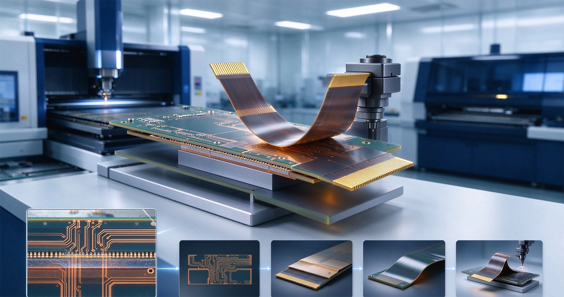
A rigid-Flex Pcb combines rigid areas, which support components and provide mechanical stability, with flexible areas, which allow folding, bending, or dynamic movement inside the final assembly. This hybrid structure introduces several manufacturing challenges that do not exist in conventional PCB production.
Unlike a standard multilayer rigid board, a rigid-flex structure must survive both the high-temperature lamination process and the mechanical stress of bending. Unlike a pure flex circuit, it must also maintain precise registration between rigid and flexible zones. That is why the manufacturing processes unique to rigid-Flex Pcb solutions require tighter process control, more specialized materials, and deeper engineering coordination.
Everything starts with the stack-up. In rigid-flex PCBs, the stack-up is not just about layer count and impedance; it also defines where the board bends, where components are placed, and how different materials bond together during lamination.
One thing that often surprises designers is how much the stack-up affects bend reliability. If the neutral axis is not properly positioned, the copper traces in the bend area may experience excessive tension or compression, which can lead to cracking over time.
Lamination is one of the most critical manufacturing processes unique to rigid-flex PCB solutions. In a standard rigid board, lamination mainly involves bonding multiple FR-4 layers together. In rigid-flex, the manufacturer must bond rigid materials, flex materials, and sometimes adhesive films into a single reliable structure.
During lamination, temperature, pressure, and vacuum level must be carefully controlled. Too much pressure can squeeze adhesive into flex areas and reduce flexibility. Too little pressure can cause Delamination or voids. The process window is narrower than for ordinary rigid PCBs, which is why experienced suppliers matter a lot here.
Another important point is that flex layers are usually laminated only in specific zones. The areas that need to remain flexible must be protected from rigid prepreg flow. Manufacturers often use special layup techniques, such as localized stiffeners or controlled resin flow materials, to keep the flex region free of rigid material.
Drilling rigid-flex boards is more difficult than drilling standard rigid PCBs because the drill must pass through materials with very different mechanical properties. Polyimide flex layers behave differently from FR-4 cores, and this can affect hole quality, smear, and plating uniformity.
Manufacturers typically use specialized drill parameters for rigid-flex boards, including adjusted spindle speed, feed rate, and entry/backup materials. Microvias are also common in high-density rigid-flex designs, especially when space is limited in wearable devices, medical instruments, or aerospace electronics.
Routing and profiling are equally important. Rigid-flex boards are often cut into complex shapes, with separate rigid islands connected by flex tails. The outline must be defined precisely to avoid damaging flex circuits during depaneling. Laser cutting, mechanical routing, and punch tools may all be used depending on the design.
The bend area is where rigid-flex PCBs really show their value, and also where many failures happen if the process is not handled correctly. Before bending, the flex layers must be properly prepared to reduce stress on copper traces.
Coverlay application is a key step here. Coverlay protects flex circuits the way solder mask protects rigid boards, but it also adds mechanical support. The coverlay openings must align accurately with pads and vias, otherwise soldering defects or exposure issues may occur.
Good design practice for bend areas includes:
In one project involving a handheld medical scanner, the initial prototype failed a bend test because several ground traces ran straight across the flex hinge. After rerouting those traces in an arc pattern and moving nearby vias outward, the board passed repeated bending tests without issues. Small changes like that can make a huge difference.
Surface finish selection for rigid-flex PCBs requires extra care. The finish used on rigid areas may not be suitable for flex areas. For example, ENIG is commonly used on rigid sections because it provides a flat surface for fine-pitch components. However, the flex areas usually remain covered by polyimide coverlay, so the surface treatment strategy must be defined separately for each zone.
Impedance Control is also more challenging in rigid-flex designs. The dielectric thickness, copper width, and reference planes can change between rigid and flex regions. Manufacturers must measure and control impedance based on the actual stack-up in each area, not just assume a uniform structure across the entire board.
Testing typically includes:
Because rigid-flex boards are often used in high-reliability applications, manufacturers may also perform cross-section analysis, peel strength testing, and moisture resistance testing depending on customer requirements.
Even the best manufacturer cannot fully compensate for a poorly designed rigid-flex board. Early collaboration between design engineers and the PCB supplier can prevent many problems.
Here are some practical recommendations:
Also, remember that rigid-flex boards usually cost more than rigid-only boards. But when they replace multiple connectors, cables, and separate PCBs, the total system cost and assembly complexity can actually go down. That is one reason rigid-flex remains attractive despite its higher unit price.
It depends on the material, copper thickness, and whether the bend is static or dynamic. For static bends, the minimum radius is often around 6 to 10 times the total flex thickness. For dynamic bending, it may need to be larger. Always confirm with your manufacturer.
Yes, but Impedance Control and Material Selection become more important. The transition between rigid and flex areas should be designed carefully to avoid signal discontinuities.
Rigid-flex boards can range from simple 2-layer structures to complex multilayer designs with 10 or more layers. However, more layers increase manufacturing difficulty and cost.
Static flex means the board is bent once during assembly and remains in that position. Dynamic flex means the board bends repeatedly during product use, such as in folding devices or moving mechanisms. Dynamic flex requires more careful material and trace design.
The manufacturing processes unique to rigid-flex PCB solutions make these boards more demanding than standard rigid or flex-only circuits. From Stack-up Design and hybrid lamination to bend area preparation and specialized testing, each step requires careful planning. But when done correctly, rigid-flex technology can greatly improve product reliability, reduce assembly complexity, and enable compact designs that would otherwise be impossible.
If you are considering rigid-flex for your next project, start by discussing your bend requirements, layer structure, and application environment with your PCB manufacturer early. A little engineering alignment upfront can save significant time and cost during production.
Understanding Metal Core PCBs (MCPCB) for Superior Thermal ManagementJuly/13/2026
Why Choose Rigid-Flex PCB Solutions for Complex Industrial Assemblies?June/17/2026

Thermal Resistance and Dielectric Layers in Metal Core PCB SolutionsOctober/12/2026
Minimizing Signal Loss and Crosstalk in High-Speed PCB LayoutsSeptember/01/2026
How Heavy Copper Solutions Improve Reliability in Motor DrivesSeptember/16/2026

Tailored Industrial PCB Solutions for Medical Device ManufacturersJune/12/2026

Innovative Industrial PCB Solutions for Renewable Energy SystemsAugust/11/2026
Custom Industrial PCB Solutions for the Automotive SectorMay/27/2026