

High-speed Pcb Design demands meticulous attention to Signal Integrity, where picosecond timing margins leave no room for compromised electrical performance. Signal loss attenuates communication amplitudes while crosstalk corrupts adjacent channels, together creating failure modes that defy traditional Pcb Design approaches. This article presents comprehensive strategies for minimizing signal loss and crosstalk through stack-up planning, routing techniques, and Material Selection optimized for high-speed applications including 5G communications, data center interconnects, and automotive radar systems.
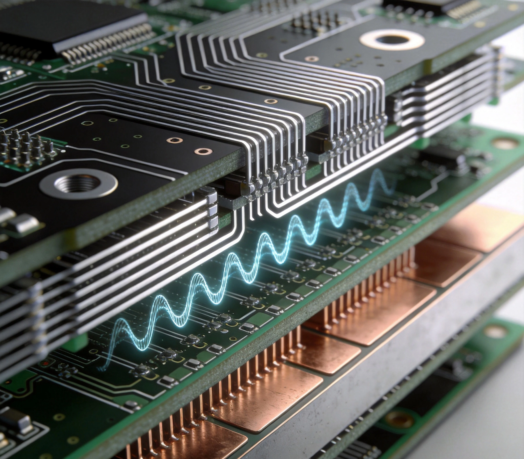
Signal loss in PCBs arises from multiple mechanisms that transform electrical energy into unwanted heat or radiated emissions. Conductor losses dominate at lower frequencies, resulting from the inherent resistance of copper traces. At high frequencies approaching gigahertz ranges, Skin Effect forces current to flow along conductor surfaces, effectively reducing cross-sectional area and increasing effective resistance. Surface Roughness exacerbates Skin Effect losses, with rough copper interfaces increasing attenuation by 10-30% compared to smooth plated traces.
Dielectric losses represent the second major contributor, arising from energy dissipation within Pcb Substrate materials as alternating signals polarize molecular structures. Loss tangent (Df) quantifies this dissipation, with lower values indicating better high-frequency performance. Standard FR4 materials exhibit Df values of 0.02-0.03, while high-performance substrates like Rogers Ro4003c provide Df below 0.004—a sevenfold improvement in dielectric loss characteristics.
Via transitions introduce discontinuities that degrade signal quality through impedance mismatches. Through-hole vias create stub effects when length exceeds signal wavelength quarter-wavelength, causing resonant behavior that selectively attenuates specific frequencies. Back-drilled vias remove unused barrel sections, eliminating stubs while maintaining ground connections through carefully controlled drill depth and plating specifications.
Controlled Impedance routing maintains consistent trace impedance throughout signal paths, preventing reflections that distort waveform shapes. Single-ended traces typically target 50Ω impedance for standard interfaces, while Differential Pairs aim for 100Ω or 90Ω depending on protocol specifications. Achieving Controlled Impedance requires precise Stack-up Design combining trace geometry with dielectric material properties.
Microstrip routing on outer layers provides accessible controlled impedance paths with predictable field distribution. Reference planes beneath traces establish return paths, with plane distance primarily determining characteristic impedance. Wider traces reduce impedance for fixed dielectric thickness, enabling impedance tuning through width adjustment during layout. Manufacturing tolerances of ±10% on trace width require tolerance stacks that may limit achievable impedance accuracy.
Stripline configurations route signals between internal reference planes, providing superior isolation from external interference and environmental factors. Symmetric Stripline constructions maintain consistent impedance regardless of surface Solder Mask or component loading. Asymmetric configurations enable mixed impedance routing within single layers, accommodating diverse interface requirements without stack-up complexity.
Differential signaling provides inherent noise rejection essential for high-speed interfaces including USB, PCIe, and Ethernet. Differential Pairs transmit complementary signals along paired traces, with receivers extracting information from voltage differences rather than absolute levels. This approach cancels common-mode noise while doubling effective signal swing, enabling higher data rates across lossy channels.
Pair spacing critically determines differential impedance and coupling characteristics. Tight coupling with spacing equal to trace width produces highly coupled pairs occupying minimal routing area. Loose coupling with 2-3x width spacing simplifies manufacturing tolerance requirements while providing greater flexibility in impedance targeting. Most protocols specify coupling requirements, with USB 3.0 requiring tight coupling while SATA permits loose routing.
Length matching between pair members prevents skew that degrades receiver discrimination. Skew introduces timing offsets between complementary signals, reducing effective noise margin and limiting maximum data rates. Length matching tolerances typically target 0.127mm (5mil) for DDR interfaces and tighter 0.025mm (1mil) for high-speed serial links. Meandering traces achieve length matching while maintaining controlled spacing throughout serpentine sections.
Effective Stack-up Design establishes foundations for Signal Integrity before routing begins. Layer sequencing positions critical signal layers adjacent to solid reference planes, establishing clean return paths and minimizing loop inductance. Power planes serve as references when properly decoupled, though slotting or absence creates discontinuities requiring careful management. Consistent plane assignment across board area prevents impedance variations that accumulate along signal paths.
Prepreg selection determines dielectric properties experienced by Microstrip traces. Standard prepregs like FR4 offer acceptable performance up to 2-3GHz, beyond which specialized materials provide necessary loss reduction. Hybrid stack-ups combining standard and high-performance materials balance cost against performance requirements, with critical high-speed layers assigned to premium substrates while lower-frequency routing utilizes economical materials.
Via-in-pad constructions create low-inductance connections for BGA escape routing but introduce discontinuities requiring compensation. Non-conductive via fill eliminates clearance issues while plated via barrels maintain electrical connectivity. Back-drilling removes unused stub sections from through-hole vias, with typical stub lengths below 0.38mm (15mil) sufficient for data rates to 10Gbps. Laser Microvias provide stub-free transitions in HDI constructions, enabling bandwidths exceeding 25Gbps.
Crosstalk arises from electromagnetic coupling between adjacent conductors, with energy transferring through capacitive and inductive pathways. Capacitive coupling injects currents into victim traces proportional to voltage rates of change, while inductive coupling induces voltages proportional to current rates of change. Both mechanisms intensify with higher frequencies and tighter routing geometries, making crosstalk particularly problematic in high-speed digital designs.
Forward crosstalk propagates in the same direction as aggressor signals, with coupled energy adding constructively over extended parallel runs. This phenomenon scales with coupled length, making long parallel segments particularly vulnerable. Backward crosstalk propagates toward signal sources, with magnitude determined by coupling coefficient and victim line termination. Both types require management through spacing and shielding strategies.
Guard traces positioned between aggressor and victim nets provide electrostatic shielding that reduces capacitive coupling. Grounded traces between high-speed signals create barriers that attenuate field penetration into adjacent routing channels. Effectiveness improves with reduced spacing to aggressors and continuous ground connections through stitching vias at regular intervals.
Trace geometry determines field distribution and coupling characteristics throughout signal paths. Width selection balances Impedance Control against routing density, with narrower traces reducing coupling at the cost of higher resistance and manufacturing sensitivity. Spacing between traces directly controls coupling magnitude, with 3W spacing (three times trace width) providing approximately 70% crosstalk reduction compared to 1W spacing.
Orthogonal routing on adjacent layers minimizes coupling between crossing traces. Electric fields align perpendicular to conductor surfaces, so traces crossing at right angles couple minimally despite perpendicular orientation. Layer assignment strategies route critical signals on dedicated layers with reference planes, reserving other layers for less sensitive routing where moderate crosstalk introduces acceptable risk.
Avoidance routing designates exclusion zones around critical nets, preventing proximity that would introduce coupling. Design rules specify minimum clearances from sensitive nets to other routing, with rule values calibrated against expected board density and performance requirements. Automated routing tools apply these rules during placement, though manual routing provides greater control over critical signal paths.
Signal return paths significantly influence high-speed signal behavior, with reference plane continuity essential for clean signal integrity. Current flows beneath conductors in reference planes, with field concentration creating impedance determined by geometry. Any interruption in reference plane creates discontinuities that degrade signal quality through impedance mismatches and mode conversion.
Plane slots and splits introduce discontinuities when signal routes across boundaries between different reference potentials. Crossing these boundaries requires stitching capacitors or stitching vias that maintain return current paths around splits. ferrite beads or explicit common mode filters may provide additional filtering for sensitive applications. Careful layer planning often eliminates problematic crossings by routing signals on layers referencing appropriate planes throughout their paths.
Via stitching establishes return paths for signals crossing reference boundaries through adjacent ground vias that bypass discontinuities. Via placement within 2-3 trace widths of signal vias ensures effective bypass, with spacing beyond this range providing diminishing returns. Differential pairs require matched via placement maintaining symmetry throughout transitions, with odd-mode impedance effects requiring careful management during paired via transitions.
Substrate materials determine dielectric losses and dimensional stability affecting high-speed performance. Rogers and Panasonic substrates provide lower loss tangents than standard FR4, with Rogers RO3003 offering Df of 0.001 and RO4003C providing 0.003 at 10GHz. These materials command premium pricing but enable longer transmission distances and higher data rates that justify additional cost for demanding applications.
Thermal expansion coefficients (CTE) influence reliability during temperature cycling, with mismatch between substrate and copper creating mechanical stress on plated through-holes. High-tg Materials reduce CTE-related fatigue, with Tg values above 170°C providing improved thermal stability. For lead-free assembly processes with higher reflow temperatures, materials with Tg exceeding 260°C prevent glass transition issues that compromise board integrity.
Moisture absorption affects Dielectric Constant stability, with hydrophilic materials experiencing permittivity shifts as humidity varies. Polyimide substrates resist moisture absorption better than polyetherimide alternatives, maintaining consistent impedance over environmental ranges. Desiccant storage and bake-out procedures minimize moisture-related defects during assembly, with moisture sensitivity level (MSL) ratings guiding handling requirements.
Time-domain reflectometry (TDR) characterizes impedance discontinuities throughout signal paths, identifying problems before they impact system performance. TDR instruments inject fast rise-time pulses into traces, measuring reflections that reveal impedance variations with millimeter resolution. This testing validates prototype designs and production samples, verifying manufacturing consistency across production lots.
Vector network analysis (VNA) provides frequency-domain characterization including Insertion Loss, return loss, and crosstalk measurements across operating frequency ranges. These measurements correlate with eye diagram performance for digital signals, enabling prediction of link budgets and margin assessments. VNA testing validates channel compliance against interface specifications including USB, HDMI, and PCIe requirements.
Eye diagram analysis summarizes overall channel quality through overlay of accumulated bit patterns, revealing timing jitter, amplitude noise, and intersymbol interference. Clear eye openings indicate adequate margin for reliable communication, while closed eyes signal performance limitations requiring design optimization. Statistical eye analysis quantifies performance distributions across manufacturing samples, enabling correlation with Accelerated Life Testing for Reliability Prediction.
Effective design rules codify signal integrity requirements into enforceable layout constraints.规则 capture coupling limits, spacing requirements, and geometry specifications derived from simulation and measurement correlation. Rules tailored to specific product requirements balance performance against routing density, with tighter constraints on critical nets and relaxed requirements for lower-priority signals.
Stack-up rules define layer assignments and material specifications ensuring manufacturing consistency. Impedance targets with associated tolerances establish baseline parameters for controlled impedance traces. Dielectric thickness and material property specifications ensure fabrication houses deliver boards matching design intent. Clear stack-up documentation prevents misinterpretation that leads to impedance mismatches.
Routing rules specify trace geometry, spacing, and via usage for different signal categories. High-speed serial links receive strict constraints on differential pair spacing, length matching, and via usage. Power delivery networks follow separate rules addressing current capacity and thermal considerations. Partitioning rules prevent sensitive analog circuits from coupling with noisy digital switching circuitry.
electromagnetic simulation tools predict signal behavior before prototype fabrication, enabling optimization without costly iterations. 2D field solvers calculate trace impedance and coupling based on geometry and material properties, verifying stack-up designs before manufacturing. 3D full-wave simulators model complex structures including connectors, vias, and component packages that 2D tools cannot accurately capture.
Channel simulation connects component and trace models into complete signal paths, predicting eye diagrams and compliance margins for given data rates and signal amplitudes. Statistical simulation accounts for manufacturing variations, revealing performance distributions across tolerance stacks. This analysis identifies robust designs that perform reliably across manufacturing and environmental ranges rather than designs that pass nominal conditions but fail corners.
Power integrity simulation analyzes PDN impedance and switching noise effects on signal performance. VRM modeling, decap placement optimization, and plane resonance prediction enable PDN designs that minimize supply noise coupling to sensitive circuits. Combined signal and power integrity simulation reveals interactions between power and signal domains, enabling holistic optimization rather than isolated domain management.
Signal integrity success requires collaboration between design teams and manufacturing partners. Fabrication specifications communicate stack-up requirements, material selections, and impedance targets that ensure manufactured boards match design intent. Dielectric thickness tolerances and copper weight specifications establish acceptable ranges that fabricators can achieve while maintaining Impedance Control.
Design For Manufacturing (DFM) feedback identifies layout features that may challenge production capabilities. Fine trace spacing, controlled impedance tolerances, and via structures require specific manufacturing capabilities that not all fabricators provide. Early engagement with qualified manufacturers prevents design decisions that exceed production capabilities, avoiding costly respins when manufacturing limitations surface during qualification testing.
Test vehicle development validates manufacturing process capability for high-speed designs. Test coupons on production panels characterize impedance uniformity, coupling characteristics, and via performance across board locations. These measurements verify that production processes deliver performance matching design intent and simulation predictions, with statistical process control maintaining capability throughout production runs.
Minimizing signal loss and crosstalk in High-speed Pcb layouts demands systematic attention to stack-up design, routing geometry, Material Selection, and manufacturing collaboration. Signal loss mechanisms including conductor loss, dielectric loss, and via discontinuities require mitigation through appropriate material choices, controlled impedance design, and via optimization techniques. Crosstalk management combines spacing rules, guard traces, and orthogonal routing to maintain signal isolation throughout critical paths.
Successful High-speed Pcb design integrates simulation-driven validation with manufacturing collaboration, ensuring designs are both electrically optimal and producible. Design rules capturing best practices enable consistent signal integrity across engineering teams, while test and measurement verification validates compliance with interface specifications and performance requirements. These practices enable reliable high-speed products that perform consistently across manufacturing and environmental ranges.
As data rates continue increasing in 5G, datacenter, and automotive applications, signal integrity discipline becomes increasingly essential. Designs meeting today's requirements may fail tomorrow's higher-speed protocols, demanding continuous attention to emerging specifications and manufacturing capabilities. Engineering teams investing in signal integrity expertise and simulation infrastructure position themselves to address evolving requirements while maintaining competitive product development schedules.
Why Choose Rigid-Flex PCB Solutions for Complex Industrial Assemblies?June/17/2026

Innovative Industrial PCB Solutions for Renewable Energy SystemsAugust/10/2026
Reducing Weight and Space with Rigid-Flex Industrial PCB SolutionsJuly/28/2026
Manufacturing Challenges in 20+ Layer Industrial PCB SolutionsJuly/09/2026
An Introduction to HDI Technology for Compact Industrial ElectronicsJune/16/2026
Aluminum vs. Copper Base: Choosing the Best Metal Core SolutionJuly/29/2026
Stack-up Design Strategies for High-Layer Count Industrial PCBsOctober/09/2026

Cost Analysis: Is Rigid-Flex the Right Solution for Your Industrial Project?September/15/2026