Open Nav


As PCB designs move into higher frequency ranges, surface roughness becomes one of the most underestimated factors affecting Signal Integrity. At low frequencies, copper roughness has little practical impact. But as signal edge rates increase and operating frequencies reach multi-gigahertz levels, the interaction between current distribution and conductor surface texture begins to influence insertion loss, impedance, phase response, and overall channel performance.
This article explains how surface roughness affects high-speed signals, why the skin effect makes roughness more important at higher frequencies, how roughness is modeled in simulation, and what PCB designers can do to manage it without unnecessarily increasing cost.
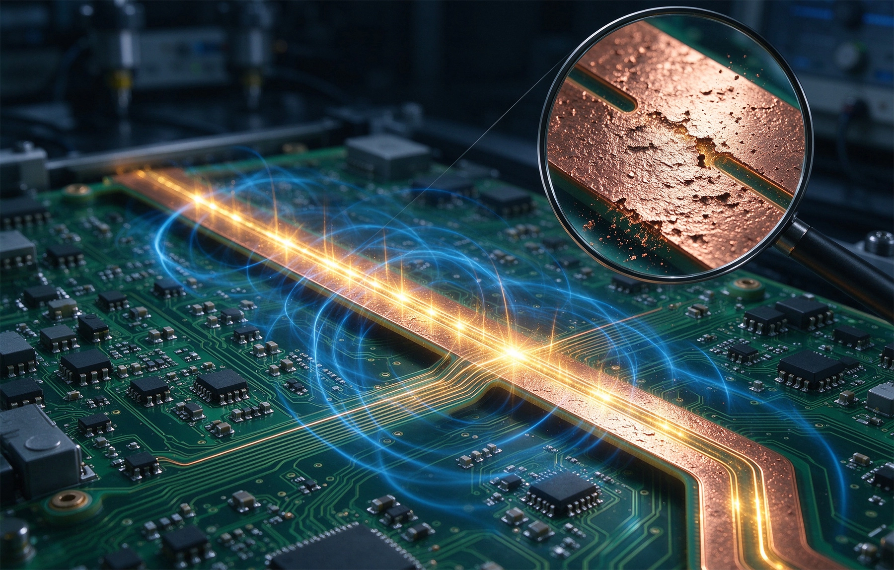
High-speed signals do not travel through the entire cross-section of a copper conductor. Due to the skin effect, current concentrates near the surface of the trace as frequency increases. The skin depth decreases with frequency, which means the effective conduction region becomes thinner and closer to the copper surface.
When the copper surface is rough, the current path becomes longer and less uniform. Instead of flowing along a smooth boundary, the electromagnetic field interacts with peaks, valleys, and nodules on the copper surface. This increases the effective resistance of the conductor and raises conductor loss.
The result is higher insertion loss, especially in the high-frequency portion of the spectrum. For serial links, backplanes, RF circuits, high-speed digital buses, and mmWave designs, this can reduce eye height, increase jitter, and limit achievable data rates.
Conductor loss in a PCB trace comes from two main sources: the bulk resistance of copper and the additional loss caused by surface texture. At low frequencies, bulk resistance dominates. At high frequencies, surface-related effects become significant.
Rough copper increases loss through several mechanisms:
In many high-speed channels, conductor loss and dielectric loss both matter. However, once a low-loss laminate is selected, copper roughness can become the dominant variable in conductor loss. Using ultra-low-loss material with very rough copper may not deliver the expected performance improvement.
Not all copper foils behave the same way. PCB manufacturers choose copper foil based on adhesion, cost, process compatibility, and electrical performance.
Electrodeposited, or ED, copper is widely used in standard PCBs. It typically has higher surface roughness because the Plating Process creates a grain structure with noticeable peaks and valleys. ED copper provides good mechanical adhesion to dielectric materials, but it is less ideal for very high-frequency designs unless treated or smoothed.
Reverse-treated foil is a variation of ED copper in which the rough side is treated to improve bonding while the drum side remains smoother. This allows designers to orient the smoother surface toward the signal trace when the stackup permits. It is a practical compromise between adhesion and Signal Integrity.
Rolling-annealed, or RA, copper is produced by mechanical rolling and annealing. It generally has lower surface roughness and better high-frequency performance. RA copper is often used in Flexible Circuits and high-reliability RF applications, but it may cost more and is not always available for standard rigid PCB processes.
Modern high-speed laminates often support very low profile, or VLP, and ultra-low profile, or HVLP, copper foils. These foils reduce surface roughness while maintaining acceptable peel strength. For 10G, 25G, 56G, and higher-speed channels, VLP and HVLP foils are frequently specified to control insertion loss.
Surface roughness is usually described using parameters such as Ra, Rz, and Rq. Ra is the arithmetic average roughness. Rz represents average peak-to-valley height over a sampling length. Rq is the root-mean-square roughness. These values are useful for comparing foils, but they do not fully describe the three-dimensional shape of the surface.
In Pcb Design, the most important question is not the roughness number alone, but how that roughness affects signal loss at the target frequency. Two foils with similar Ra values may behave differently because their peak distribution, nodular structure, and bonding treatment are not identical.
For simulation, engineers often use empirical roughness models rather than raw roughness measurements. Common models include the Hammerstad model, the Huray model, and the Cannonball model. These models estimate an effective increase in resistance based on surface texture. They are not perfect, but they help bridge the gap between material data and channel simulation.
The most visible impact of surface roughness is increased insertion loss. As roughness increases, the attenuation per unit length rises, especially at higher frequencies. For a long backplane or high-density interconnect, this can reduce the usable bandwidth of the channel.
In time-domain performance, higher conductor loss reduces eye height and may increase deterministic jitter. The channel behaves like a stronger low-pass filter, which slows edge rates and reduces signal amplitude. If the design already has tight loss budgets, rough copper can push the channel below the required margin.
Roughness does not only affect amplitude. It can also affect phase response because the effective propagation constant changes slightly when the current distribution is disturbed. In Differential Pairs, asymmetric roughness between the two conductors may contribute to mode conversion, although this effect is usually smaller than loss and skew caused by geometry or dielectric variation.
Surface roughness is not always a design-limiting factor. For low-speed digital circuits, power boards, or short traces, standard copper foil is usually acceptable. The impact becomes significant when several conditions appear together.
Roughness should be considered carefully when:
If a design uses standard FR-4 and operates below 1 GHz, roughness is rarely the primary concern. If a design targets 25 Gbps or higher over several inches, roughness may need to be specified explicitly.
Do not wait until fabrication to consider copper type. If the channel loss budget is tight, specify low-roughness foil such as VLP or HVLP during the stackup definition stage. This allows the fabricator to choose compatible materials and processes.
Wider traces have lower conductor loss, but they also affect impedance and routing density. For controlled-impedance designs, work with the fabricator to balance trace width, dielectric thickness, and copper weight. Sometimes a small change in dielectric height reduces loss more effectively than changing copper foil alone.
Low-loss laminates reduce dielectric loss, but they do not eliminate conductor loss. The best results usually come from combining low-loss material with smooth copper. If only one change is possible, evaluate which loss component dominates at the target frequency.
High-speed channel simulation should include a roughness model. Without it, simulated insertion loss may look optimistic. Apply Hammerstad, Huray, or vendor-provided models based on measured material data. Then compare simulation with TDR, VNA, or channel test results to calibrate the model.
Ask laminate suppliers for Dk, Df, and roughness-related parameters at relevant frequencies. Generic datasheet values are useful for early estimation, but production-grade designs benefit from measured data tied to specific material grades and copper types.
For critical designs, include test coupons with different copper foils, trace widths, and lengths. Measure insertion loss and compare it with simulation. This feedback loop helps refine future stackups and reduces the risk of overdesign or underdesign.
Lower roughness is not always better for every application. Very smooth copper can reduce peel strength and increase the risk of Delamination if the laminate system is not optimized. HVLP foils may cost more and may not be available for every layer count or board thickness.
The goal is not to minimize roughness everywhere, but to apply it where it matters. For example, high-speed signal layers may use low-profile copper while power planes and mechanical layers use standard foil. This targeted approach helps control cost without sacrificing performance.
Roughness also affects high-speed digital channels. Modern serial links operate with frequency content well into the multi-gigahertz range, where conductor loss becomes significant.
Reducing dielectric loss helps, but it does not fix conductor loss. If copper roughness dominates, changing only the laminate may not deliver the expected improvement.
Ra provides a simple comparison, but simulation models usually require additional parameters. Relying only on Ra can lead to inaccurate loss prediction.
Smooth copper reduces conductor loss, but it must be compatible with the lamination process. If adhesion fails, reliability problems will outweigh electrical benefits.
Surface roughness has a measurable impact on high-speed signal integrity because it increases conductor loss, modifies effective impedance, and reduces channel margin at higher frequencies. As data rates continue to increase, copper foil selection becomes as important as dielectric Material Selection. However, roughness should be managed through informed tradeoffs rather than blanket rules.
For practical Pcb Design, the best approach is to define the loss budget early, choose appropriate copper foil for critical signal layers, include roughness models in simulation, and validate results with measured data. When these steps are applied consistently, surface roughness becomes a controlled design parameter instead of a hidden source of performance loss.
Not significantly. At low frequencies, current distributes more evenly through the conductor, so surface roughness has minimal impact on loss.
Hammerstad and Huray models are commonly used. The best choice depends on the available material data and the frequency range of the design.
HVLP copper reduces conductor loss, but it may cost more and requires compatible lamination processes. It should be used where the loss budget justifies it.
Yes, indirectly. Roughness changes the effective current distribution and field confinement near the conductor surface, which can slightly affect impedance and phase response.
If simulated insertion loss is close to the channel budget and the design operates at multi-gigahertz frequencies, include a roughness model and compare it with smooth-copper assumptions. A large difference indicates that roughness should be specified explicitly.

How to Implement a Robust Quality Assurance Plan for Industrial PCBsJuly/07/2026
Understanding IPC Class 3 Standards for High-Reliability Industrial PCBsJune/11/2026
Environmental Stress Screening (ESS) for Validating Industrial PCB QualityAugust/08/2026
Identifying and Fixing Micro-Vias Issues in Industrial PCB Quality InspectionsSeptember/10/2026
Why Electrical Testing is Non-Negotiable for Industrial PCB QualitySeptember/29/2026
Essential Quality Control Tests for Industrial PCBs- ICT, FCT, and AOIMay/27/2026
The Role of Flying Probe Testing in Industrial PCB Quality ControlJuly/22/2026
Overcoming Common Defects in Industrial PCB FabricationAugust/03/2026