Open Nav


Designing a 4-layer PCB stack-up is relatively straightforward. Signal layers on the outside, ground and power planes inside—done. But when you're building Industrial Electronics that require 12, 16, or even 24 layers, the stack-up becomes an engineering decision with real consequences for Signal Integrity, power distribution, manufacturability, and cost.
High-layer count stack-ups aren't just more layers of the same thing. They require deliberate architecture—deciding which layers carry which signals, where planes go, how power domains are distributed, and how the whole construction balances electrical performance against manufacturing reality. Get it right, and your design performs reliably. Get it wrong, and you'll chase Signal Integrity problems, power delivery issues, and manufacturing defects that could have been prevented.
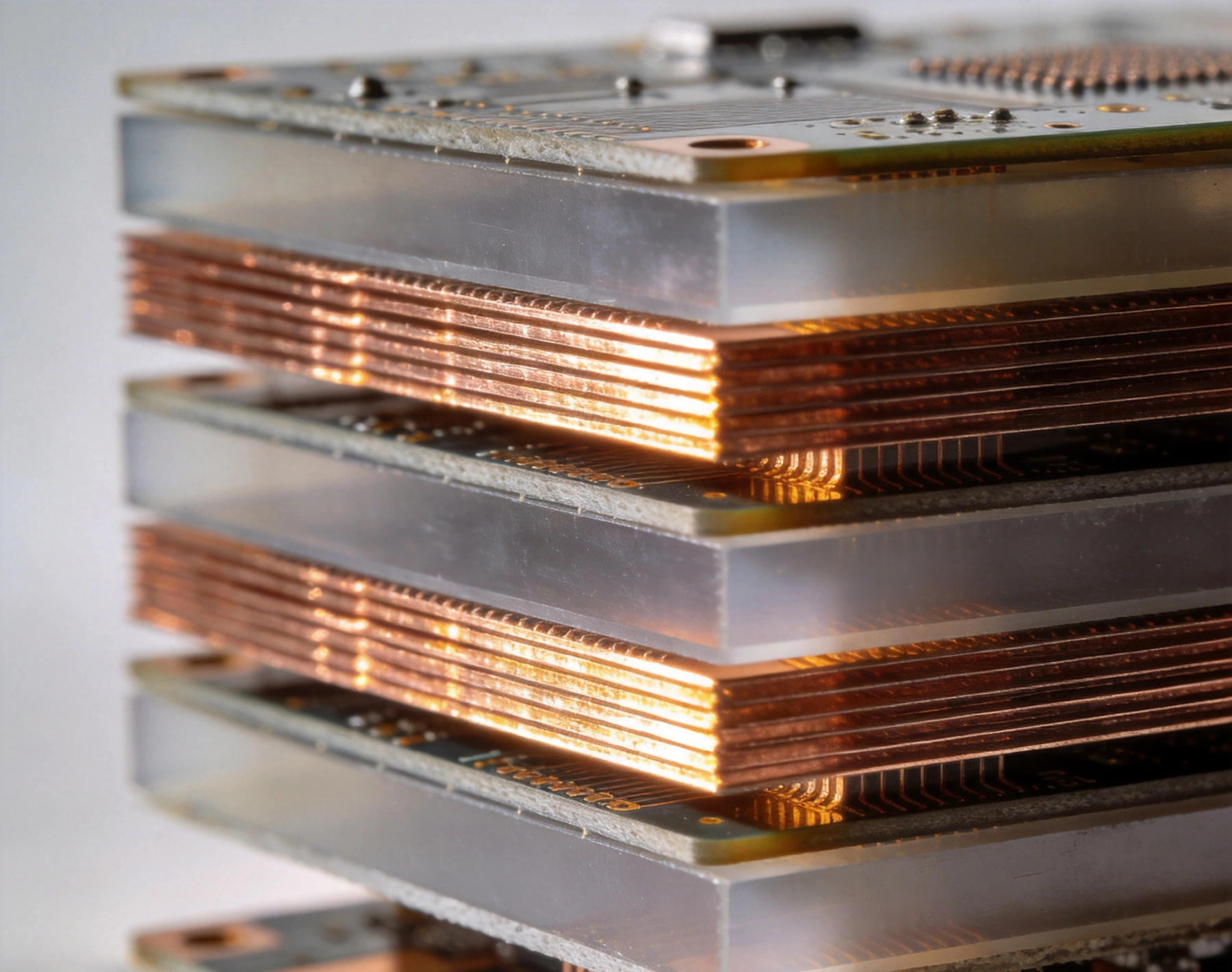
At low layer counts, the stack-up options are limited and the electrical implications are relatively simple. A 4-layer board has two signal layers and two planes—there aren't many ways to arrange them. As layer count increases, the number of possible arrangements grows, and the consequences of each choice compound.
On a 16-layer board, you're making decisions about where to place high-speed signals versus low-speed control logic, how many ground planes you need and where they go, how to distribute multiple power rails across available plane layers, and how to maintain impedance control across signal layers with different reference planes. Each decision affects the others, and poor choices interact badly.
The stack-up also determines manufacturing complexity and cost. An asymmetrical stack-up may warp during lamination. Uneven copper distribution across layers causes similar problems. Via structures—through-hole, blind, or buried—depend on which layers need to connect and how the stack-up is built up. These manufacturing considerations aren't afterthoughts—they're constraints that the stack-up must satisfy from the beginning.
Regardless of layer count, certain principles apply to all well-designed stack-ups:
Every signal layer should have an adjacent ground or power plane as its reference. This provides return current path, controls impedance, and reduces crosstalk between signal layers. When a signal layer doesn't have an adjacent reference plane, return currents find longer paths, increasing loop area, inductance, and EMI radiation.
In practice, this means alternating signal and plane layers: signal, ground, signal, power, signal, ground, and so on. This arrangement ensures every signal layer has a nearby reference. The specific spacing between signal and reference layers determines the impedance of traces on that signal layer.
A symmetrical stack-up—where the layer arrangement from top to bottom mirrors the arrangement from bottom to top—prevents warpage during lamination and soldering. Copper distribution, dielectric thickness, and material types should be balanced across the board's central plane.
Asymmetrical stack-ups sometimes seem electrically convenient, but the manufacturing problems they cause are real. Warped boards don't fit in enclosures, cause assembly alignment issues, and can develop cracked solder joints under Thermal Cycling. The electrical convenience is rarely worth the manufacturing grief.
Ground planes provide return current paths and Emi Shielding. Power planes distribute supply voltage. Both provide reference for signal layers, but they're not interchangeable. A signal referenced to a power plane has a different return current path than one referenced to ground—the return current must find a path through decoupling capacitors to reach ground, adding inductance.
For high-speed signals, ground-referenced layers are preferred. Power planes serve as references for less critical signals, or when the signal switching is referenced to that particular power rail. The stack-up should place the most critical signals on ground-referenced layers and use power-referenced layers for signals that tolerate the additional return path inductance.
Several proven patterns work well for high-layer count industrial boards:
For boards dominated by high-speed signals, the signal-ground pattern provides the best signal integrity. Each signal layer is paired with an adjacent ground layer. On a 16-layer board, this might look like: Signal, Ground, Signal, Power, Ground, Signal, Ground, Signal (core), Signal, Ground, Signal, Power, Ground, Signal, Ground, Signal.
This pattern maximizes the number of ground-referenced signal layers and provides excellent impedance control and crosstalk performance. The trade-off is that it consumes layers for ground planes that could otherwise carry signals or additional power rails. Boards with many power domains or limited layer budgets may need to compromise.
For boards with many power domains—common in industrial systems with multiple voltage rails—a modified pattern allocates more layers to power distribution. Power planes are paired, with each pair splitting a layer between two voltage domains using split planes.
Split planes work on inner layers where routing doesn't cross the splits. Each power domain occupies a region of the plane layer, separated by gaps that prevent shorting between domains. The splits must be wide enough to prevent arcing at the operating voltage, and signals on adjacent layers shouldn't route across splits, which would disrupt their return current path.
The most critical signals—clocks, high-speed Differential Pairs, sensitive analog—benefit from being sandwiched between two reference planes. This Stripline configuration provides the best crosstalk isolation and Emi Shielding, because the signal is enclosed on both sides by reference planes.
On high-layer count boards, reserving a few internal signal layers for critical signals in Stripline configuration is worthwhile. Less critical signals can use Microstrip (one reference plane) on outer or near-outer layers. This tiered approach puts the most sensitive signals in the best electrical environment while using outer layers for signals that don't need as much protection.
Different signal layers in the stack-up may require different impedance targets. A DDR4 interface needs 40-ohm single-ended and 85-ohm differential impedance. A USB 3.0 interface needs 90-ohm differential. A generic digital signal might target 50 ohms single-ended. Each of these requirements constrains the trace geometry and layer spacing on the signal layer where that interface resides.
The stack-up must be designed so that each signal layer can achieve its required impedance with trace widths that are manufacturable. If a 50-ohm trace on an internal layer requires 3-mil width due to tight spacing to the reference plane, that's a manufacturability problem—3-mil traces yield poorly and cost more. Adjusting the dielectric thickness to allow wider traces at the target impedance is the right approach.
Dielectric thickness between signal and reference layers determines the trace width needed for target impedance. Thinner dielectrics require narrower traces for the same impedance; thicker dielectrics allow wider traces. For manufacturing yield, wider traces are better.
However, thinner dielectrics provide better crosstalk performance—the tight coupling to the reference plane reduces the distance over which signals can interfere. The design must balance impedance manufacturability against crosstalk performance.
A practical approach: use tighter spacing (thinner dielectrics) for the most critical, highest-speed signal layers where crosstalk is the primary concern. Use more relaxed spacing for less critical signals where manufacturability dominates. Most high-layer count stack-ups use a mix of dielectric thicknesses optimized for the signals on each layer.
Industrial boards often need many power rails: 3.3V, 5V, 12V, 1.8V, 1.2V, and various analog supply voltages. Distributing these across the available plane layers requires planning.
Each power rail can have its own dedicated plane layer, or multiple rails can share a layer through split planes. Dedicated planes provide the best power distribution—lowest impedance, best decoupling performance—but consume layer real estate. Split planes are more layer-efficient but have higher impedance at the split boundaries and require careful routing discipline on adjacent signal layers.
For high-current power rails (1.8V core supply feeding an FPGA, or 12V motor drive power), dedicated planes are worth the layer cost. The low impedance improves transient response and reduces voltage ripple. For low-current rails (a 3.3V rail feeding a few I/O buffers), split planes are usually adequate.
On high-layer count boards, unused areas of signal layers can be filled with copper connected to power or ground. This copper fill provides additional decoupling capacitance between layers and improves thermal performance. However, copper fill must be managed carefully—randomly connected copper islands can create resonant structures that amplify noise at specific frequencies rather than reducing it.
The best practice is to fill unused areas with ground-connected copper, using consistent connection patterns (via arrays at regular intervals) that prevent floating islands. Power-connected fill should only be used where the fill is clearly associated with a specific power domain and doesn't create coupling paths between domains.
Via structures interact closely with the Stack-up Design. The choice between through-hole, blind, and buried vias depends on which layers need to connect and how the stack-up is constructed.
Through-hole vias penetrate all layers. They're the simplest and cheapest via type, but they create anti-pads (clearance holes) on every layer they pass through. On a 20-layer board, a through-hole via creates an anti-pad on 18 layers it doesn't connect to, consuming routing space on each of those layers.
At high layer counts, the routing blockage from through-hole vias becomes significant. Signal layers lose routing channels to via anti-pads, creating congestion that may force wider trace spacing or additional layers. This is one reason why high-layer count boards often benefit from blind and buried vias despite their added cost.
Blind Vias connect an outer layer to one or more inner layers without passing through the entire board. Buried vias connect between inner layers without reaching either surface. Both types reduce anti-pad blockage on layers they don't traverse, freeing routing space.
The stack-up determines which blind and Buried Via configurations are manufacturable. Sequential Lamination builds the board in multiple steps, with vias created between specific layer subsets at each step. Not all via configurations are possible with all stack-up constructions—the fabricator's process capabilities constrain what you can do.
Design the stack-up with the fabricator's capabilities in mind from the beginning. Finding out after layout that your via strategy isn't manufacturable is an expensive problem. Finding out before layout starts is a planning conversation.
High-layer count industrial boards often dissipate significant power. The stack-up affects thermal performance in several ways:
Internal copper planes spread heat laterally across the board. More continuous plane layers provide better heat spreading. A stack-up with fragmented planes or many signal layers without solid copper references will develop hotter spots than one with robust plane coverage.
The layer position of heat-generating components matters. Components on outer layers can conduct heat directly to heat sinks or the enclosure. Components connected to inner-layer planes benefit from the plane's heat spreading but can't directly couple to external cooling. The stack-up should place the most critical power components where thermal performance is best.
Thermal Vias—small vias under component pads that connect to internal planes—provide a path for heat to reach the spreading layers. Their effectiveness depends on the number of vias, their diameter, and the Thermal Conductivity of the internal planes they connect to. A well-designed Thermal Via array can significantly reduce component junction temperature.
Before committing a high-layer count stack-up to production, verify these manufacturing requirements:
Lamination registration: Can the fabricator maintain layer-to-layer registration across all layers at your required accuracy? Registration error accumulates with layer count—a 20-layer board has more registration risk than a 6-layer board.
Copper balance: Is the copper distribution approximately symmetric about the board center? Large imbalances cause warpage. Small local imbalances (a signal layer with different routing density than its mirror) are usually acceptable, but gross asymmetry is not.
Dielectric material consistency: Are all dielectric layers specified with appropriate material grades? Mixing high-Tg and standard-Tg materials in the same stack-up is sometimes necessary but creates differential thermal expansion that can cause reliability problems.
Via aspect ratio: Are all drilled holes within the fabricator's aspect ratio capability? High layer counts mean thicker boards, and thicker boards with small holes create high aspect ratios that may exceed drilling and plating capability.
At minimum, two ground planes on either side of the core provide basic return current paths. For good signal integrity on a signal-dense 16-layer board, 4 to 6 ground planes are typical—one for every two to three signal layers. The exact number depends on your signal density, speed, and crosstalk requirements.
Yes, this is common in hybrid stack-ups where some layers carry high-frequency signals requiring low-loss materials while others use standard FR-4. The materials must be compatible in lamination temperature and thermal expansion. Your fabricator should confirm that the material combination is processable and reliable.
Each additional layer pair adds roughly 15 to 25 percent to the board fabrication cost, depending on complexity and volume. Additional layers also increase lamination cycles (if blind/buried vias are involved), drilling time, and testing complexity. The cost justification depends on whether the additional layers solve problems that would be more expensive to fix through other means.
It depends on routing density. If through-hole vias provide adequate routing space, they're simpler and cheaper. If routing congestion from through-hole anti-pads forces wider spacing or additional layers, Blind Vias may actually reduce total cost by allowing fewer total layers or smaller board dimensions.
Engage your fabricator early—before layout begins. Provide your proposed stack-up and via strategy, and ask them to confirm manufacturability, flag any concerns, and suggest alternatives if needed. This conversation is far cheaper than discovering problems after layout is complete.
Contact us to discuss your requirements.
How Heavy Copper Solutions Improve Reliability in Motor DrivesSeptember/16/2026

Tailored Industrial PCB Solutions for Medical Device ManufacturersJune/12/2026

Overcoming Bend Radius Challenges in Flex PCB SolutionsAugust/14/2026
Understanding Metal Core PCBs (MCPCB) for Superior Thermal ManagementJuly/13/2026
Minimizing Signal Loss and Crosstalk in High-Speed PCB LayoutsSeptember/01/2026
Material Selection Guide for High-Speed Industrial PCB SolutionsJuly/14/2026
Manufacturing Processes Unique to Rigid-Flex PCB SolutionsOctober/10/2026
Thermal Resistance and Dielectric Layers in Metal Core PCB SolutionsOctober/12/2026