Open Nav


As Industrial Pcb assemblies grow more complex — finer pitch BGAs, QFN packages with large center thermal pads, double-sided placement, and high-density interconnects — the fraction of solder joints that cannot be seen by any optical method keeps increasing. On a modern industrial board, 40-60 percent of solder joints may be hidden from view. Automated optical inspection (Aoi) and manual visual checks are powerless against these concealed connections. Only X-ray inspection can see through the component body and the Pcb Substrate to evaluate the solder joint beneath.
For complex Industrial Pcba projects — motor drives, power converters, PLC modules, medical instruments, and avionics — the cost of an undetected solder defect is not just a board failure. It is field downtime, warranty claims, safety liability, and reputational damage. X-ray inspection is not a luxury for these applications; it is a necessity. This article explains why X-ray is vital, what defects it detects that other methods cannot, how 2D and 3D X-ray differ, and what you should require from your assembly partner's X-ray capability.
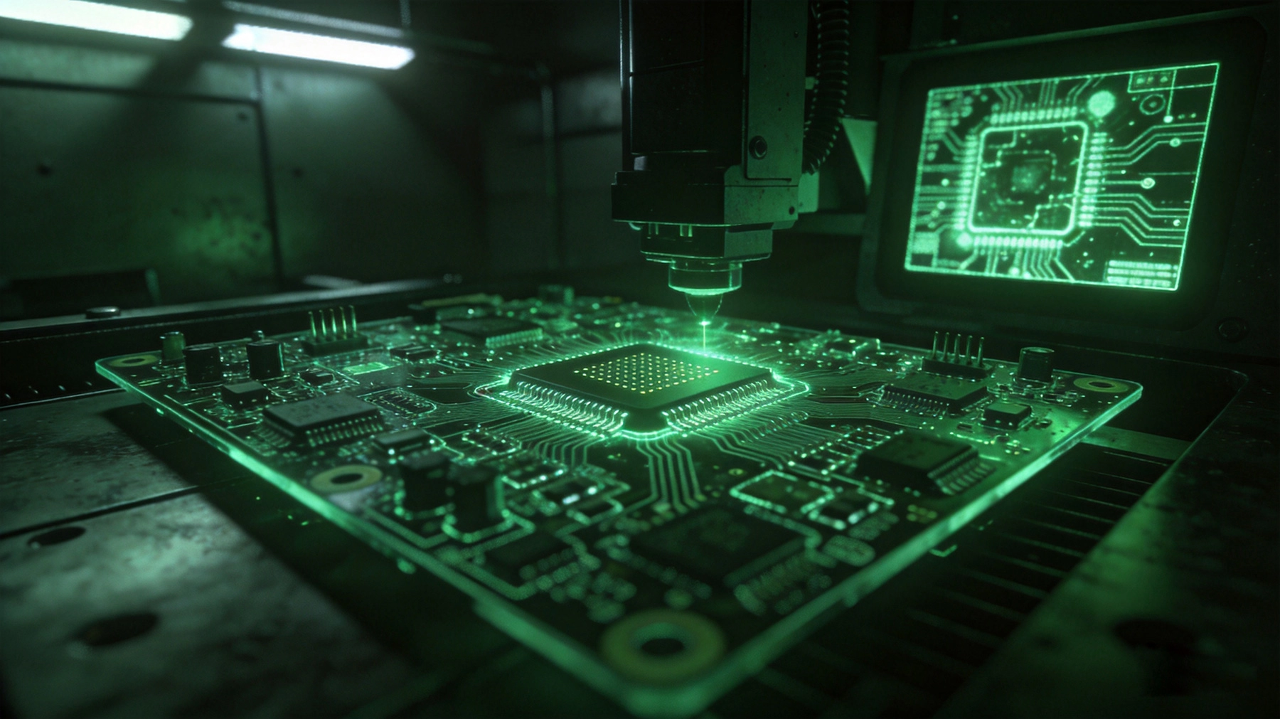
The fundamental limitation of optical inspection is line of sight. If a solder joint is physically obscured — by the component body, by adjacent components, or by the board itself — no camera, no matter how high its resolution, can evaluate it. The proliferation of area-array packages has made this the norm rather than the exception.
On a typical industrial power board with a BGA microcontroller, several QFN power stages, and an LGA sensor, the hidden joint count can easily exceed 500. Without X-ray, every one of those joints is an unverified assumption.
X-ray inspection reveals the internal structure of solder joints — the joint volume, shape, wetting, void content, and positional accuracy. These characteristics are invisible to Aoi and critical to joint reliability.
Voids are cavities within the solder joint formed by gas entrapment during reflow — outgassing from flux, moisture in the paste, or air trapped during stencil printing. Voids reduce the effective cross-section of the joint, increasing electrical resistance and thermal resistance. In power applications, voids in the thermal pad of a QFN power stage directly degrade Heat Dissipation, potentially pushing the device above its rated junction temperature.
IPC-A-610 sets void area limits — typically 25 percent maximum for Class 2 and 20 percent for Class 3 (military, aerospace, medical) on BGA balls. For thermal pads, some specifications require even tighter limits (5-15 percent) because of the thermal performance impact. Only X-ray can measure void area and distribution within the joint.
Solder bridging between adjacent BGA balls or QFN pads is one of the most dangerous defects because it creates a direct electrical short that can destroy components or cause latent functional failures. On fine-pitch BGAs (0.4-0.5 mm pitch), the gap between balls is small enough that even a minor excess of solder paste can create a bridge. These bridges are completely hidden under the package and produce no visual indication on the board surface.
X-ray detects bridging by showing continuous solder between ball positions. Even very thin bridges — solder filaments that are barely visible in X-ray — can be detected with proper imaging parameters.
Insufficient solder on a BGA ball results in a thin, weak joint with poor mechanical and electrical performance. Non-wetting — where the solder fails to bond to the pad or component termination — creates a joint with no metallurgical connection. Both defects are invisible from the outside on BGA and QFN packages.
X-ray reveals insufficient solder as a reduced joint diameter or height. Non-wetting appears as an irregular joint shape with a visible gap between the solder and the pad or ball, often accompanied by a characteristic dark line at the non-wetted interface.
Head-in-pillow (HiP) is a particularly insidious defect where the BGA solder ball rests on top of the solder paste deposit without coalescing — the ball and paste are in physical contact but not metallurgically joined. The joint appears to be intact from the outside (the ball is in position), but there is no electrical or mechanical connection. HiP defects are caused by stencil printing issues, paste oxidation, component warpage, or inappropriate reflow profiles.
X-ray detection of HiP requires careful observation. In 2D X-ray, the defect appears as a subtle gap or double-image effect at the ball-paste interface. In 3D X-ray (CT), the separation between ball and paste is clearly visible as a void or gap layer.
Component placement offset — where the package is shifted relative to the pad pattern — causes some joints to be soldered on reduced pad area and others to be completely off-pad. For BGA components, even a small offset (0.1 mm) can move edge balls partially off their pads, creating weak joints that fail under Thermal Cycling. X-ray reveals the positional relationship between balls and pads, showing whether the joint is centered on the pad or offset.
X-ray can also inspect internal board features — via fill quality, internal layer alignment, and Buried Via connections. For HDI boards with filled Microvias, X-ray reveals whether the via fill is complete or contains voids that could cause open circuits under thermal stress. This capability extends X-ray's value beyond assembly inspection into board-level structural verification.
X-ray inspection systems come in two fundamental types, and their capabilities differ significantly.
2D X-ray produces a single projection image — like a medical chest X-ray. The X-rays pass through the board and the image captures a shadow of everything in the beam path, superimposed into a single plane. Features on the top and bottom of the board overlap in the image.
Advantages:
Limitations:
3D X-ray acquires multiple projection images at different angles and reconstructs a volumetric model of the inspected area. This allows the operator to view any cross-sectional plane, measure true void volume (not just area), and separate overlapping features from different layers.
Advantages:
Limitations:
For most Industrial Pcba projects, 2D X-ray is sufficient for routine inspection. 3D becomes necessary when:
Manual X-ray inspection — where an operator views the image and makes accept/reject decisions — is standard for prototype and low volume builds. For production volumes, automated X-ray inspection (AXI) provides faster and more consistent defect coverage.
AXI systems use programmed inspection algorithms to automatically evaluate solder joints against predefined criteria. The system positions the X-ray source and detector over each component, acquires the image, and applies measurement algorithms to detect voids, shorts, insufficient solder, and other defects. Results are logged with position data for traceability.
X-ray inspection is not a standalone step — it integrates into the broader Quality Control flow. Understanding where it fits helps you specify your inspection requirements effectively.
For the first board off the line (or the first few boards), comprehensive X-ray inspection is standard practice. Every BGA, QFN, and LGA component is X-rayed to verify that the reflow profile, paste deposition, and placement are all producing acceptable joints. First-article X-ray catches process setup errors — wrong paste volume, incorrect reflow temperature, placement offset — before they affect the full production run.
For production boards, X-ray inspection may be performed in-line (every board) or sampling-based (a percentage of boards at defined intervals). The choice depends on the defect probability and the cost of escape:
X-ray is indispensable for Failure Analysis. When a board fails functional test, X-ray of the suspect component often reveals the root cause — a voided BGA joint, an open QFN thermal pad, or a short between fine-pitch balls. After rework (BGA reballing, component replacement), X-ray verifies that the rework joint meets acceptance criteria — a step that is often skipped but should not be, as rework joints have inherently higher defect risk than original joints.
Simply requiring "X-ray inspection" is not sufficient. You must define what the X-ray is looking for and what constitutes a defect. Key specifications include:
X-ray inspection adds cost to your assembly — equipment amortization, operator time, programming, and data storage. Understanding the return on this investment helps justify it to management.
For complex industrial PCBA projects, the ROI of X-ray inspection is overwhelmingly positive. The incremental cost of X-ray per board (typically $5-20 for manual inspection, $1-5 for AXI) is negligible compared to the cost of a single field failure.
When evaluating a PCB assembly partner for complex industrial projects, ask these X-ray-specific questions:
No. X-ray is excellent at detecting volumetric defects (voids, shorts, insufficient solder) but has limitations with some surface defects. Cold joints (poor intermetallic formation) may appear normal in X-ray if the solder volume and shape are correct, even though the metallurgical bond is weak. Crack detection in solder joints is also limited — newly formed cracks may be too fine to resolve in X-ray. X-ray should be part of a comprehensive inspection strategy that includes AOI, Ict, and functional test — not a replacement for them.
Yes, at the dose levels used for Pcb Inspection. The X-ray exposure during a typical inspection is well below the threshold that would damage electronic components, alter solder joint metallurgy, or affect board materials. The primary safety consideration is for the operator — X-ray systems are fully enclosed with interlocked shields to prevent radiation exposure.
For manual inspection of a typical industrial board with 3-5 BGA/QFN components, X-ray adds 15-30 minutes to the post-reflow inspection step. For AXI in production, the time per board is 2-5 minutes. This is a small addition to the overall build timeline and is far less than the time that would be lost if a defect is discovered later during functional test or in the field.
If your design uses only leaded components (SOT, QFP, SOIC) or two-terminal passives with visible solder fillets, AOI and visual inspection can verify all joints. X-ray adds minimal value in this case. However, if your design uses any area-array package — BGA, QFN, LGA, CSP, or PoP — X-ray is essential. The more area-array components in your design, the more critical X-ray becomes.
IPC-A-610 defines acceptance criteria for solder joints but does not mandate X-ray inspection specifically. It establishes void limits, joint dimensions, and other criteria that can only be verified with X-ray for hidden joints. The decision to perform X-ray inspection is driven by the design (hidden joints), the reliability class (Class 2 vs. Class 3), and customer-specific requirements. For Class 3 applications with BGA components, X-ray inspection is effectively required because the acceptance criteria cannot be verified any other way.
X-ray inspection is not optional for complex industrial PCBA projects — it is the only method that can verify the integrity of solder joints hidden under area-array packages. As BGA, QFN, and LGA components become standard in Industrial Electronics — power converters with QFN MOSFETs, controllers with BGA processors, sensor modules with LGA packages — the fraction of hidden joints will only increase. The cost of X-ray inspection is modest, the capabilities are mature, and the consequences of skipping it are severe. Specify X-ray inspection in your assembly requirements, define clear acceptance criteria, verify that your assembly partner has the right equipment and expertise, and insist on X-ray data in your build reports. For Industrial Electronics where reliability is non-negotiable, X-ray is not an extra — it is essential.
Contact us to discuss your requirements

SMT vs. Through-Hole: Best Practices for Industrial PCBAJuly/07/2026
Industrial PCBA: Navigating the Complexities of Box Build AssemblyJune/09/2026
Navigating the Complexities of Box Build AssemblyMay/27/2026
Manufacturing Processes for Extreme Heavy Copper Industrial PCBsAugust/15/2026
The Importance of Component Obsolescence Management in Industrial PCBAAugust/07/2026
How to Ensure Quality Control in High-Mix Low-Volume Industrial PCBAJuly/21/2026
Selective Soldering Techniques for Mixed-Technology Industrial PCBA<September/09/2026
Identifying and Fixing Micro-Vias Issues in Industrial PCB Quality InspectionsSeptember/10/2026