Open Nav


High-frequency PCBs used in industrial environments face demands that would challenge any design. Radar systems, motor drives, switching power supplies, and industrial communication equipment all push Pcb Materials and construction to their limits. A board that performs adequately at lower frequencies may exhibit serious problems when subjected to the high-speed signals and electrical stress found in demanding industrial applications. Testing and validation are not optional checkpoints but essential steps that determine whether a design will survive real-world conditions.
Too many projects treat testing as a formality to be completed after design is finished rather than an integral part of the development process. This approach works for simpler products where margins are generous and failure modes are forgiving. For high-frequency industrial PCBs, it leads to field failures that are expensive to address and potentially dangerous to ignore. Understanding what to test, how to test it, and when to test it during development makes the difference between products that work reliably and products that fail unexpectedly.
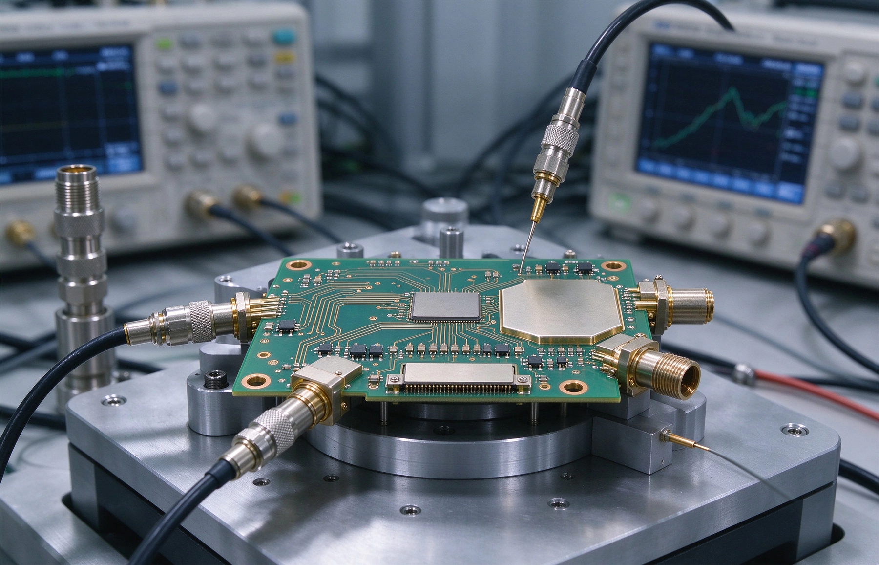
Before discussing testing methods, it helps to understand what can go wrong in high-frequency PCB applications. Different failure mechanisms dominate at different frequency ranges, and testing strategies should be designed to expose the specific failure modes relevant to your application.
Signal Integrity problems become more severe as frequency increases. Transmission Line effects that can be ignored at low frequencies become dominant concerns above approximately one gigahertz. Impedance mismatches cause reflections that distort waveforms and reduce signal fidelity. Crosstalk between adjacent traces can corrupt data in high-speed digital systems. These issues may not appear in slow-speed bench testing but manifest as intermittent failures or excessive error rates in field operation.
Thermal effects create their own category of failures in high-frequency applications. High-frequency circuits often generate significant heat through dielectric losses and conductor resistance. Over time, this heat can degrade substrate materials, weaken solder joints, and cause Delamination between layers. Boards that pass ambient temperature testing may fail when operated continuously at elevated temperatures or when Thermal Cycling causes materials to expand and contract beyond their design limits.
Electromagnetic interference affects both the board itself and nearby equipment. High-frequency signals radiate energy that can interfere with sensitive circuits or violate regulatory emission limits. Conversely, boards may be susceptible to interference from external sources like motor drives, switch-mode power supplies, or wireless transmitters. Industrial environments are notoriously electrically noisy, and designs that work in clean laboratory conditions may fail when deployed near industrial equipment.
Controlling impedance is fundamental to high-frequency Pcb Performance, and verifying that actual boards meet impedance specifications requires careful testing procedures. Impedance testing is typically performed on sample boards from each production lot to verify that the fabrication process consistently produces boards matching the design intent.
Time-domain reflectometry provides the most common method for measuring trace impedance. A TDR instrument sends a fast edge down the trace and measures reflections that occur at impedance discontinuities. By analyzing the reflection pattern, engineers can determine the trace impedance at any point along its length and identify the locations of any impedance deviations. Tdr Testing is fast enough for production testing of sample boards and sensitive enough to detect variations that would affect high-frequency performance.
Vector network analyzers offer more sophisticated impedance characterization for design validation and Failure Analysis. VNA instruments measure S-parameters that fully characterize how a trace transmits and reflects signals across a frequency range. While more expensive and time-consuming than Tdr Testing, VNA measurements provide the detailed data needed to validate simulation models and understand subtle performance issues that TDR might miss.
Differential pair testing requires additional consideration because differential impedance depends on the coupling between the two traces. Test structures must include both individual trace impedance and differential impedance measurements to fully characterize differential signaling channels. Common-mode impedance, which affects susceptibility to interference, should also be measured for applications where EMI performance is critical.
Beyond high-frequency characterization, standard electrical testing verifies basic functionality that must be correct before advanced testing is meaningful. These tests apply to all PCBs but are especially important for high-frequency designs where minor defects can have disproportionate effects.
Continuity testing verifies that all intended connections exist and no unintended shorts exist between nets. For high-frequency boards with dense routing, automated testing methods like flying probe or bed-of-nails testing provide the comprehensive coverage needed to catch subtle manufacturing defects. Manual continuity checking with a multimeter is insufficient for complex boards and misses too many potential problems.
Isolation testing measures the resistance between nets that should be electrically isolated. Low isolation resistance indicates potential problems like solder residue bridging traces, plating voids creating unexpected connections, or substrate contamination. For high-voltage applications, isolation testing is especially critical because insufficient spacing or contaminated surfaces can lead to arc discharge or tracking failures under load.
Dielectric withstanding voltage testing applies high voltage between circuits to verify that the substrate can withstand the expected voltage stress plus appropriate safety margin. This test identifies weak areas in the dielectric that might fail under transient voltage events or over time due to degradation. Industrial equipment standards often include dielectric withstanding voltage requirements that must be verified during qualification.
Industrial equipment operates in environments with significant temperature variation, and PCBs must survive these conditions without degradation. Thermal testing validates that materials and construction can withstand the expected temperature range and the Thermal Cycling that occurs during normal operation.
Continuous high-temperature exposure tests boards for extended periods at elevated temperature to identify thermal degradation mechanisms. Standard tests run for 96 to 1,000 hours depending on the reliability requirements of the application. During exposure, boards are periodically tested to track changes in electrical performance, impedance, and insulation resistance. Significant changes during exposure indicate problems that will worsen over the board's service life.
Thermal cycling tests expose boards to repeated temperature changes that cause materials to expand and contract. Each cycle stresses solder joints, plated vias, and substrate-to-copper interfaces. After a defined number of cycles, boards are tested to verify they still meet electrical specifications. The number of cycles required varies by application and environment, with industrial applications typically requiring 500 to 1,000 cycles or more. Failure during thermal cycling often manifests as increased via resistance, cracked traces, or Delamination between layers.
Thermal shock testing uses rapid temperature transitions to identify weaknesses that might not appear in slower thermal cycling. Sudden temperature changes create thermal gradients that stress materials differently than gradual transitions. This test is especially relevant for equipment that might experience sudden environmental changes or power-on thermal transients.
Industrial PCBs often face mechanical stress from vibration, shock, and physical handling. Testing for mechanical robustness ensures boards survive both during manufacturing and throughout their service life in the field.
Vibration testing applies sinusoidal or random vibration to boards while monitoring for intermittent electrical failures. The test profile should simulate the vibration environment the board will actually experience, which varies significantly between applications. Boards mounted near motors or pumps face different vibration profiles than boards in stationary industrial control cabinets. Vibration testing identifies resonance conditions that cause excessive stress and reveal weak solder joints or loose components.
Mechanical shock testing validates survivability when equipment is dropped, bumped, or subjected to sudden impact forces. For portable or mobile industrial equipment, shock testing is essential to verify that boards and their interconnections can survive the physical handling they will receive in use. Drop testing and bump testing protocols specify the shock magnitude, duration, and number of repetitions based on the expected use environment.
Humidity and moisture resistance testing addresses the reality that many industrial environments involve moisture exposure from condensation, cleaning, or humidity. Moisture can cause corrosion, dielectric breakdown, and Electrochemical Migration between traces. Boards may be tested under high humidity conditions, and some applications require boards to survive exposure to liquid water or cleaning solvents.
For high-speed digital signals, Signal Integrity testing validates that waveforms meet the requirements for reliable data transmission. Eye diagram analysis provides a comprehensive view of how actual signals behave compared to the ideal waveforms assumed during design.
Eye diagrams superimpose multiple bit periods of a digital signal to reveal the aggregate effect of all the impairments that affect signal quality. A wide, clean eye indicates good signal integrity with generous timing and voltage margins. A closed or distorted eye indicates problems that will cause data errors. Eye diagram testing is performed with high-speed oscilloscopes or dedicated signal integrity analyzers that capture enough data to build statistically meaningful diagrams.
Eye mask testing defines specific regions of the eye diagram that the signal must not enter. Standards organizations and component manufacturers specify eye masks that define minimum acceptable signal quality. Boards that produce signals meeting the mask requirements are certified to work with the corresponding receivers. Eye mask testing provides a simple pass/fail criterion for signal quality that is more objective than subjective interpretation of eye shape.
Jitter and noise analysis decompose signal quality problems into their constituent causes. Jitter, the variation in signal timing, may be caused by PLL design, power supply noise, or coupling from adjacent signals. Noise, the variation in signal amplitude, may be caused by power supply ripple, crosstalk, or reflections. Understanding the dominant impairment helps identify the root cause and guide design improvements.
Industrial products must often meet regulatory requirements for safety, emissions, and environmental impact. Testing to verify compliance protects users, avoids legal liability, and ensures products can be sold in target markets.
Electromagnetic compatibility testing verifies that boards do not generate excessive emissions and are not unduly susceptible to external interference. Regulatory requirements like FCC Part 15 for US sales or CISPR standards for international sales specify emission limits and testing procedures. EMC testing in accredited laboratories is required for certification, but pre-compliance testing during development identifies problems early when they are cheaper to fix.
Safety testing addresses hazards like electric shock, fire, and hazardous materials. Standards like UL 60950 for information technology equipment or IEC 61010 for measurement and control equipment specify requirements that must be verified through testing. For PCBs, safety testing often includes verification of spacing, insulation resistance, and flame resistance of substrate materials.
Environmental regulations like RoHS restrict the use of hazardous substances in electronics. Compliance testing verifies that components and materials meet substance restrictions and that manufacturing processes do not introduce restricted materials. Most industrial equipment customers require RoHS compliance certification, and some industries have additional environmental requirements that must be verified through testing and documentation.
No board requires every possible test, and testing everything would be prohibitively expensive. Developing an appropriate testing strategy means identifying which tests are essential for your application, which are important but optional, and which can be skipped because they do not apply to your design.
Start by identifying the environmental conditions your board will actually face. Temperature range, humidity, vibration, and electrical noise levels vary significantly between applications, and your testing should stress the board in ways that reflect real-world conditions rather than generic worst cases. Over-testing boards for conditions they will never encounter wastes money without improving reliability.
Consider the consequences of failure. A board failure in a handheld diagnostic tool has different implications than a board failure in equipment controlling industrial machinery. Higher consequences justify more thorough testing because the cost of field failures, including liability and reputation damage, far exceeds the cost of additional testing. Conversely, low-consequence applications may tolerate higher field failure rates that allow for leaner testing approaches.
Document your testing rationale and results. Clear documentation of what was tested, how testing was performed, and what results were obtained builds confidence that the board is ready for deployment. It also provides a reference for future redesigns or derivative products, where understanding what was previously tested helps focus the next round of validation.
Testing and validation for high-frequency industrial PCBs requires more comprehensive approaches than simpler board designs because the consequences of failure are more severe and the failure modes are more varied. Impedance characterization, thermal testing, mechanical validation, signal integrity analysis, and regulatory compliance testing each address different aspects of board performance that must all be acceptable for the board to succeed in its application.
The testing strategy that works best depends on your specific application, the environment your boards will face, and the consequences of failure. Building an appropriate test plan requires understanding both the testing methods available and the specific risks your design faces. Early engagement with testing considerations during design often prevents problems that would be expensive to address later.
Working with manufacturers and test laboratories that have experience in high-frequency industrial applications helps ensure that testing is performed correctly and results are interpreted appropriately. These partners can provide guidance on test methods, sample sizes, and acceptance criteria based on their experience with similar designs.
Contact us to discuss your requirements and explore testing and validation strategies for your high-frequency Industrial Pcb applications.
The Impact of Surface Roughness on High-Speed Signal IntegrityOctober/13/2026
Environmental Stress Screening (ESS) for Validating Industrial PCB QualityAugust/08/2026
Identifying and Fixing Micro-Vias Issues in Industrial PCB Quality InspectionsSeptember/10/2026
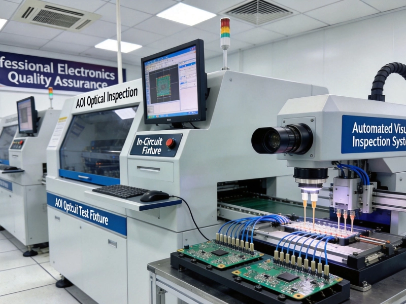
Essential Quality Control Tests for Industrial PCBs- ICT, FCT, and AOIMay/27/2026
Understanding IPC Class 3 Standards for High-Reliability Industrial PCBsJune/11/2026
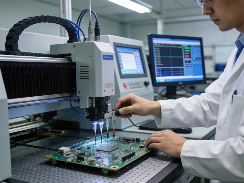
Why Electrical Testing is Non-Negotiable for Industrial PCB QualitySeptember/29/2026
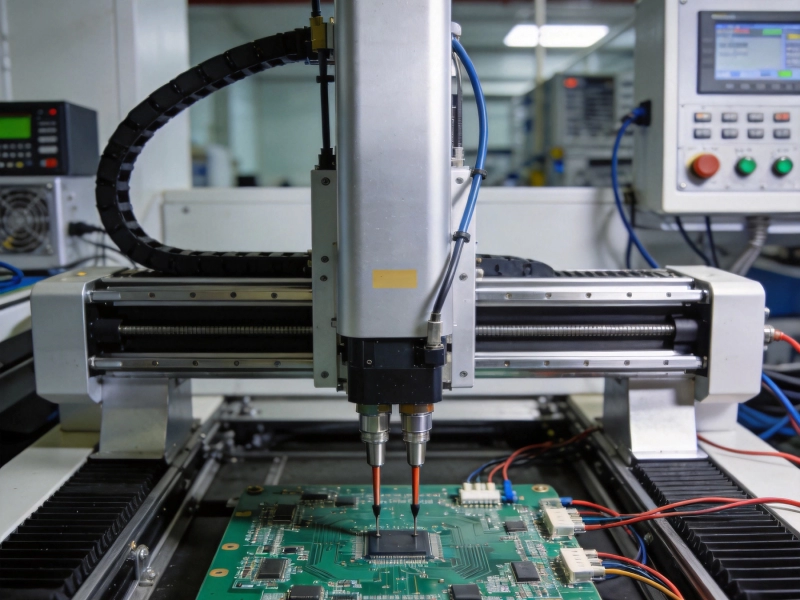
The Role of Flying Probe Testing in Industrial PCB Quality ControlJuly/22/2026
How to Implement a Robust Quality Assurance Plan for Industrial PCBsJuly/07/2026