Open Nav


High-density interconnect PCBs represent the frontier of board-level integration, and the manufacturing processes that produce them are correspondingly sophisticated. Among these processes, Sequential Lamination stands as one of the most enabling and most misunderstood techniques in modern PCB Fabrication. It is the process that makes HDI possible, and understanding how it works, when it is needed, and what its limitations are gives engineers a clearer picture of what is achievable in high-density design and what trade-offs come with each manufacturing choice.
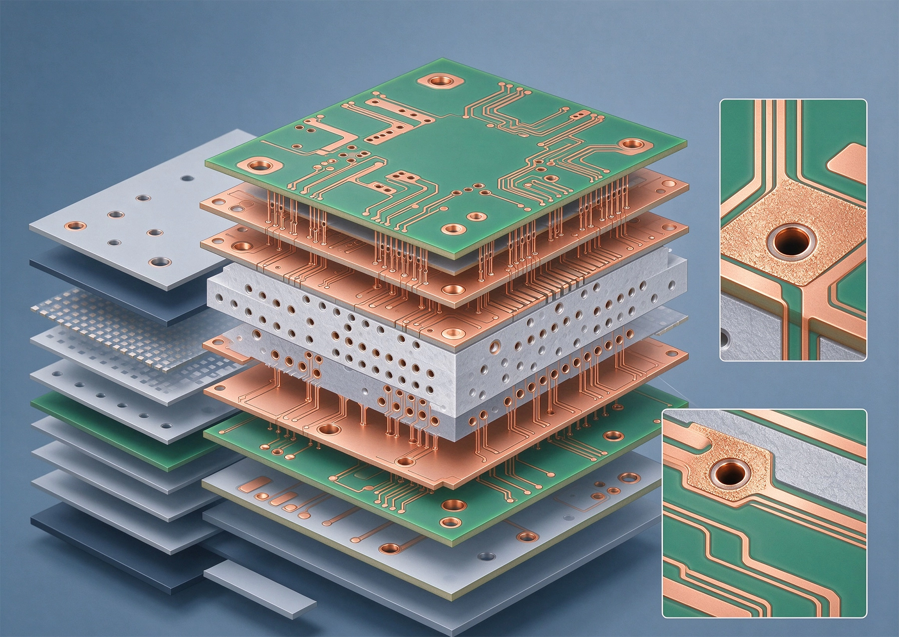
A standard Multilayer Pcb is built by laminating all layers together in a single press operation. Prepreg, the partially cured fiberglass material that acts as the adhesive and insulator between layers, flows under heat and pressure and bonds all the inner layers into a single cohesive board. This process is straightforward, reliable, and well-suited to boards where all layers are fabricated identically and the drilling happens after lamination.
Sequential Lamination breaks this process into multiple stages. Instead of building the entire board in one press operation, fabricators build it in a series of steps, where some layers are laminated, processed, and then added to in subsequent lamination cycles. This approach allows different layers to receive different treatments at different stages, which enables structural features that are impossible to produce with a single lamination step.
The most important capability that sequential lamination enables is the creation of blind and buried vias. A Blind Via, which connects an outer layer to an internal layer without traversing the full board thickness, requires that the inner layers be drilled and plated before they are covered by subsequent outer layers. A Buried Via, which connects internal layers without reaching either outer surface, requires that the layers forming the via be laminated, drilled, and plated before being covered by the outermost layers. Neither structure can be produced in a single lamination step because the via must be created before the layers above or below it exist to obstruct the drilling.
HDI designs rely heavily on Microvias: small, precisely controlled vias that connect adjacent layers with minimal land consumption. These Microvias, typically laser-drilled and less than 150 micrometers in diameter, are what allow HDI boards to achieve the routing density that sets them apart from conventional multilayer designs. The Via-in-pad construction common in HDI, where vias are placed directly in component pads rather than routed to nearby vias, depends on Microvia Technology and the sequential lamination process that makes it possible.
In a typical HDI stackup with layer-1-to-layer-2 microvias, the manufacturing sequence begins with the inner layer core, which is fabricated, drilled with any through-holes, and plated before the first lamination step. After the first lamination, the outer layers are added and laser-drilled to create the microvias that connect to the underlying core. This layered, staged construction is sequential lamination in its most common form, and it is the foundation of virtually all HDI board manufacturing.
The number of lamination cycles in an HDI board depends on the complexity of the via structure. A board with only layer-1-to-layer-2 Blind Vias may require only two lamination cycles: one to build the core and one to add the outer layers. A board with multiple microvia layers, or with complex stacking of microvias that connect through multiple dielectric layers, requires more lamination cycles, each adding cost, cycle time, and some cumulative registration challenge.
Understanding the mechanical details of sequential lamination helps engineers appreciate both its capabilities and its constraints. The process begins with the fabrication of inner layer cores, which are standard double-sided or multilayer constructions built up to a specific stage. These cores are processed through imaging, etching, and plating to create the circuit patterns and any through-hole or Buried Via structures that will be encapsulated in the final board.
After the cores are ready, they are arranged in a press tooling with prepreg and any required foil layers, and the first lamination cycle is performed. The temperature, pressure, and dwell time in this cycle are carefully controlled to ensure complete cure of the prepreg without damaging the circuitry on the cores. After lamination, the panel is inspected and any necessary drilling is performed. For HDI boards, this drilling is typically Laser Drilling for microvias, though mechanical drilling may also be used for larger buried vias.
Following drilling, the newly created vias are plated to create the electrical connections between layers. The Plating Process for microvias must achieve good step coverage: the electroless copper that initiates the plating must coat the walls of the microvia completely, including the bottom corner where the via meets the underlying pad, which is the most challenging geometry to cover uniformly. This is followed by electrolytic copper plating to build the final conductor thickness.
Subsequent lamination cycles repeat this pattern with additional cores and prepreg layers. Each cycle adds layers and may create additional via structures between the newly added layers and the previously built structure. The complexity of the stackup determines how many cycles are required, and each cycle adds cost because it is a discrete manufacturing step with its own setup, labor, and cycle time.
If there is a single technical challenge that defines sequential lamination, it is registration: the ability to align features from one lamination cycle to the next with the precision required for reliable circuitry. Every time a board goes through a lamination cycle, the prepreg flows and the core layers shift slightly under pressure. These shifts are small, typically measured in tens of microns, but they are significant relative to the tolerances required for fine-pitch components and dense microvia arrays.
Fabricators manage registration through a combination of tooling design, process control, and inspection. Panel fiducials are established before the first lamination and are used to track layer positions through subsequent cycles. Cross-sectional analysis of production samples verifies that the registration is within specification. For high-precision HDI work, some fabricators use scan-and-correct systems that measure actual layer positions after each lamination cycle and generate adjusted drill files for subsequent cycles to compensate for measured offsets.
The cumulative registration error across multiple lamination cycles limits how many sequential lamination steps are practical in a given board design. While a well-controlled two-cycle sequential lamination process can achieve registration tolerances of plus or minus 75 microns or better, adding more cycles increases the cumulative error budget. Designs that require very fine microvia-to-pad registration, such as those targeting 130-micron or finer pitch BGA packages, typically need to minimize the number of lamination cycles and may need to use more sophisticated registration correction techniques.
Sequential lamination is not always the optimal manufacturing approach, and understanding when it is warranted versus when it adds unnecessary complexity is an important design decision. The clearest indicator is the via structure of the design. If the design requires Blind Vias, buried vias, or any via that does not traverse the full board thickness, sequential lamination is necessary. There is no alternative process that can produce these structures in a single lamination step.
HDI designs almost universally require sequential lamination because their defining feature is the use of microvias in combinations that include blind structures. A typical HDI design with two or more microvia layers, stacked microvias, or any form of Via-in-pad construction cannot be manufactured without sequential lamination. The decision is not whether to use sequential lamination but how many lamination cycles are needed and how to optimize the stackup to minimize them.
Beyond HDI, sequential lamination is sometimes used for non-HDI designs that benefit from its other capabilities. Boards with very high layer counts, where the fabrication sequence for buried vias and complex routing makes sequential processing more controllable, sometimes benefit from staged lamination even if no microvias are involved. Boards with mixed dielectric requirements, where different layers need different material properties, can sometimes use sequential lamination to incorporate different materials at different stages. These are more specialized applications, but they illustrate that sequential lamination's utility extends beyond HDI in specific scenarios.
The stackup design for a board that will be manufactured with sequential lamination requires different thinking than the stackup for a standard multilayer board. The stackup is not just a list of dielectric thicknesses and copper weights; it is also a manufacturing sequence that must be feasible, cost-effective, and capable of achieving the required tolerances.
One of the key stackup decisions is the number of lamination cycles. Each additional lamination cycle adds cost and some registration risk, so the goal is to achieve the required layer connectivity with the minimum number of cycles. A stackup that achieves all required layer connections in two lamination cycles is preferable to one that requires three or four, all else being equal. The stackup designer must understand the via structures required and work backwards to determine the minimum lamination sequence that can produce them.
Material Selection also interacts with the lamination sequence. High-frequency materials like Rogers laminates, which have different thermal expansion characteristics than standard FR-4, may behave differently under the multiple lamination cycles of a sequential process. The fabricator must understand how the chosen materials will respond to sequential lamination and may need to adjust process parameters like temperature and pressure to achieve good results. This is another reason why early engagement with the fabricator on stackup design is valuable.
Via structures in the stackup should be planned to minimize the complexity of the lamination sequence. For example, a design that uses only layer-1-to-layer-2 microvias has a simpler lamination requirement than one that also includes layer-2-to-layer-3 microvias, which would require a three-cycle lamination. Where the electrical requirements allow, designing the via structure to use the most straightforward lamination sequence reduces cost and improves manufacturability.
Sequential lamination adds cost to PCB Fabrication because it adds manufacturing steps. Each lamination cycle incurs setup cost, material cost, labor overhead, and cycle time that a single-lamination board does not have. The incremental cost per additional lamination cycle varies by fabricator and by the specific board complexity, but it is not trivial; a board that requires three lamination cycles instead of one can carry a cost premium of 50 percent or more compared to an equivalent single-lamination design.
The most effective cost management strategy for sequential lamination starts at the design stage. Designs that require fewer lamination cycles cost less to manufacture. Designs that use standard materials and processes rather than exotic combinations cost less. Designs that target standard panel sizes and fabrication capabilities rather than requiring custom tooling cost less. The design decisions that minimize lamination complexity are often invisible to the designer who is not aware of the manufacturing process, which is why early collaboration with the fabricator on stackup design pays off.
Beyond the lamination count, the cost of sequential lamination is influenced by the precision requirements of the design. Tighter registration tolerances require more sophisticated tooling, more inspection, and potentially more rework, all of which add cost. Designs that specify registration tolerances tighter than the fabricator's standard process capability will incur a premium. Understanding what tolerances are actually required by the components and routing of your design, versus what tolerances are simply specified because they sound good, helps avoid over-specifying and overpaying.
The complexity of sequential lamination makes the fabricator relationship more important than it is for standard multilayer boards. Not all PCB fabricators have sequential lamination capability, and among those that do, the range of capabilities and the quality levels achieved vary significantly. Identifying a fabricator with the specific sequential lamination capabilities your design requires, and engaging them early in the design process, is one of the most practical steps a design team can take.
Early engagement typically starts with sharing the design intent: the target layer count, the required via structures, the stackup constraints, and the registration tolerances driven by the component pitches in the design. The fabricator can then advise on stackup options that meet the electrical requirements while minimizing lamination complexity, identify any material or process constraints that should influence the design, and provide design rules that reflect their actual manufacturing capabilities rather than generic industry guidelines.
Design reviews at key milestones, before and after release of the stackup and before release of the production files, help catch manufacturability issues early when they are inexpensive to correct. A fabricator who understands the design intent can often suggest design modifications that improve manufacturability without affecting electrical performance. These suggestions are most valuable early in the process, before design changes become disruptive.
Sequential lamination is the enabling technology behind virtually all Hdi Pcb solutions and a range of other advanced multilayer designs. By allowing boards to be built in multiple stages, it creates the possibility of blind vias, buried vias, and the dense microvia structures that make modern high-density interconnect designs practical. The trade-off is added manufacturing complexity, additional cost, and tighter constraints on registration and process control.
The key to successful use of sequential lamination is understanding its capabilities and limitations well enough to make informed design decisions. Designers who understand how the process works can create stackups that achieve the required connectivity with the minimum lamination complexity. They can specify tolerances that are genuinely needed rather than defaulting to unnecessarily tight values. They can engage their fabricators early enough to benefit from their process expertise, rather than discovering manufacturability issues after the design is finalized. This understanding does not require deep manufacturing expertise; it requires awareness of what sequential lamination enables and what it costs, applied at the design stage where that awareness has the most impact.
Contact us to discuss your requirements.
Why Choose Rigid-Flex PCB Solutions for Complex Industrial Assemblies?June/17/2026
Rogers vs. PTFE: Comparing Materials for High-Frequency SolutionsSeptember/17/2026

Cost Analysis: Is Rigid-Flex the Right Solution for Your Industrial Project?September/15/2026
Stack-up Design Strategies for High-Layer Count Industrial PCBsOctober/09/2026
Manufacturing Challenges in 20+ Layer Industrial PCB SolutionsJuly/09/2026
End-to-End Industrial PCB Solutions: From Design to DeliveryJuly/08/2026
Via-in-Pad and Microvias: Key Features of Advanced HDI SolutionsJuly/26/2026

Cost-Effective Industrial PCB Solutions for IoT ApplicationsSeptember/11/2026