Open Nav


In the realm of advanced electronics, the demand for miniaturization and higher circuit density is relentless. Industrial applications, from aerospace avionics to medical imaging devices, require Printed Circuit Boards (PCBs) that can pack immense processing power into shrinking footprints. Traditional mechanical drilling, while robust, has hit a physical limitation when it comes to creating the microscopic interconnections required for these high-density designs. This is where The Role of Laser Drilling in High-Precision Industrial PCB Fabrication becomes pivotal.
Laser drilling has revolutionized the way we create vias—specifically Microvias—in modern PCBs. Unlike mechanical drills, which are limited by the physical diameter and fragility of the drill bit, lasers use concentrated light energy to ablate material with extreme precision. In this article, I will explore the mechanics of laser drilling, its specific applications in industrial PCBs, and why it is the cornerstone of High Density Interconnect (HDI) technology.
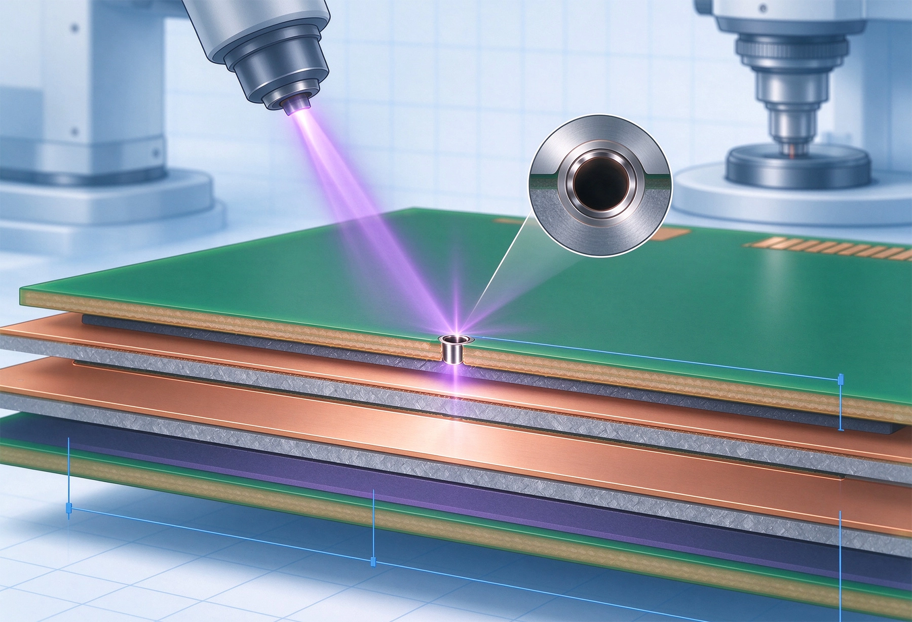
Laser drilling for PCBs primarily utilizes two types of laser systems: CO2 lasers and UV (Ultraviolet) lasers. Understanding the difference is key to understanding their role in fabrication.
CO2 lasers are the workhorses of the industry, primarily used for drilling through dielectric materials (resin and glass fiber) to expose underlying copper pads. They operate at a wavelength of roughly 10.6 micrometers. The process involves the laser beam heating the dielectric material until it vaporizes (ablates), leaving a clean hole. However, CO2 lasers cannot penetrate copper; therefore, they require an existing "capture pad" of exposed copper to stop the drilling process.
UV lasers operate at a much shorter wavelength (355 nm), allowing for a smaller spot size and higher precision. Unlike CO2 lasers, UV lasers can ablate both dielectric materials and copper. This makes them essential for drilling into copper-clad surfaces or for creating extremely small Microvias in rigid-flex and flexible PCBs. The "cold ablation" process of UV lasers minimizes the heat-affected zone (HAZ), reducing the risk of damaging the surrounding substrate.
Industrial Electronics operate in harsh environments and demand higher reliability than consumer gadgets. The shift toward laser drilling is driven by several critical factors inherent to The Role of Laser Drilling in High-Precision Industrial PCB Fabrication.
Industrial control boards and military computers often require complex signal routing. Mechanical drills generally cannot create holes smaller than 150 micrometers (6 mils) reliably. Laser drilling, however, can consistently produce microvias as small as 25-50 micrometers. These microvias allow for finer trace widths and spacing, enabling designers to route more signals in less space, which is the definition of Hdi Technology.
In high-frequency industrial applications (like radar systems or 5G infrastructure), Signal Integrity is paramount. Mechanical through-holes often create long "stubs"—unused portions of the via barrel that act as antennas, reflecting signals and causing data loss. Laser-drilled blind and buried vias are much shorter and can be stacked or staggered. This reduces parasitic inductance and capacitance, ensuring cleaner signal transmission at high speeds.
Many industrial sensors and robotics utilize rigid-flex PCBs to fit into complex 3D shapes. Mechanical drilling exerts physical force (down-thrust) which can distort flexible polyimide materials. Laser drilling is a non-contact process, eliminating mechanical stress and ensuring that delicate flex circuits remain flat and undamaged during fabrication.
Laser drilling is not a standalone step; it is part of a sequence. Once the laser creates the via, the hole walls are often left with resin smear or carbonized debris (especially in FR-4 materials). This is where the desmear process becomes critical. Chemical or plasma treatments are used to clean the hole walls and expose the inner copper layers. Without effective desmear, the subsequent copper plating will not adhere properly, leading to "head-in-pillow" defects or open circuits. Understanding this interplay is a subtle but vital part of The Role of Laser Drilling in High-Precision Industrial Pcb Fabrication.
While powerful, laser drilling introduces its own set of challenges:
As Industrial Electronics continue to evolve toward higher speeds and smaller form factors, the limitations of mechanical drilling become increasingly apparent. Laser drilling offers the precision, versatility, and reliability needed to manufacture the next generation of HDI and rigid-flex boards. By mastering The Role of Laser Drilling in High-Precision Industrial Pcb Fabrication, manufacturers can push the boundaries of what is possible in electronic design, ensuring that critical industrial systems perform flawlessly.
UV lasers can drill holes as small as 15-20 micrometers, while CO2 lasers typically bottom out around 50-75 micrometers. This is significantly smaller than the practical limit of mechanical drilling (~150 micrometers).
CO2 lasers cannot drill through copper; they reflect off it. UV lasers, however, can ablate copper, allowing them to drill through thin copper foils or create vias in copper-clad substrates.
For individual holes, lasers are extremely fast (milliseconds per hole). However, mechanical drills can drill multiple holes in a stack (panelization). For large, simple through-holes, mechanical is faster. For thousands of tiny microvias, laser is the only viable option.

Eco-Friendly Practices in Modern Industrial PCB FabricationSeptember/20/2026
The Impact of Surface Finishes on Industrial PCB Fabrication QualityJuly/16/2026
Precision Engineering: Tolerances in High-End Industrial PCB FabricationSeptember/03/2026
Advanced Techniques in Multi-Layer Industrial PCB FabricationJune/03/2026
Overcoming Common Defects in Industrial PCB FabricationAugust/03/2026
Predicting Lifespan: Accelerated Life Testing for Industrial PCB ReliabilityAugust/03/2026
How to Choose the Right Manufacturer for Industrial PCB FabricationJune/29/2026
Materials, Methods, and Industry Standards ExplainedMay/27/2026