Open Nav


The electronics industry has an environmental footprint that is easy to overlook and hard to shrink. A single square meter of finished PCB has consumed roughly 200 liters of water, 25 kWh of electricity, and grams of heavy metals by the time it ships—and the global industry produces hundreds of millions of square meters per year. The etching, plating, lamination, and soldering processes that define PCB Fabrication are inherently resource-intensive, relying on strong acids, metal salts, organic solvents, and high-temperature presses. But that is changing. Driven by regulation, customer mandates, and genuine corporate responsibility, eco-friendly practices in industrial PCB Fabrication have moved from aspirational to operational—reducing environmental impact while maintaining (and often improving) product quality and cost competitiveness.
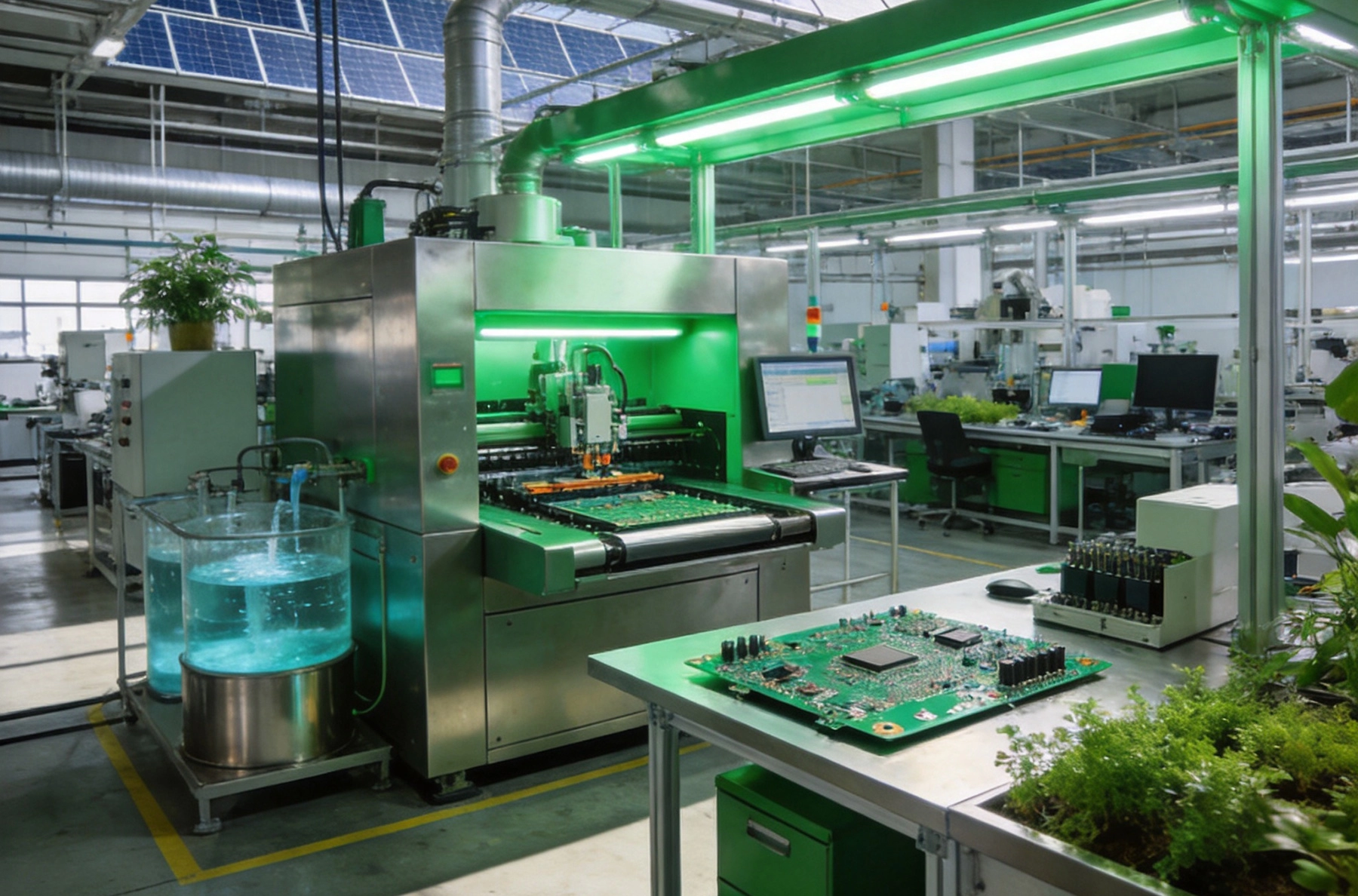
Understanding where the impact occurs is the first step toward reducing it. The major environmental burdens of Pcb Fabrication are:
Every one of these burdens has a viable reduction strategy—and in many cases, the strategy also reduces cost. Environmental efficiency and economic efficiency are not enemies; they are often the same thing.
The transition from tin-lead (Sn63Pb37) to lead-free solder alloys—driven by the EU RoHS directive and now adopted globally—is the single most impactful eco-friendly change in PCB history. Lead is a persistent, bioaccumulative toxin; removing it from solder eliminates the largest single source of heavy-metal contamination in electronics end-of-life.
The dominant lead-free alloy, SAC305 (Sn96.5Ag3.0Cu0.5), has been in volume production since 2006. Its environmental benefits are clear:
But SAC305 is not without environmental trade-offs. Silver and tin mining have their own environmental impacts, and the higher reflow temperature (~250 °C vs. ~220 °C for SnPb) increases energy consumption per board by roughly 10–15 %. Newer low-temperature lead-free alloys (Sn42Bi58, Sn89Zn8Bi3) are emerging that reflow at 180–200 °C, reducing energy use—though their long-term reliability in industrial applications is still being validated.
Water is the lifeblood of Pcb Fabrication—and its biggest waste stream. Modern eco-friendly fabs implement a multi-tier water strategy:
Instead of single-pass rinse tanks that drain continuously, closed-loop systems recirculate rinse water through ion-exchange columns that remove dissolved metals and ions. The purified water returns to the rinse tank; the ion-exchange columns are regenerated periodically, producing a small volume of concentrated metal-bearing solution that is sent to metal recovery. Water consumption drops by 80–90 % compared to single-pass rinsing.
In a counter-current rinse cascade, fresh water enters only the final (cleanest) rinse stage and flows backward through successive stages, each slightly more contaminated than the next. The workpiece moves in the opposite direction—through the dirtiest rinse first and the cleanest last. This arrangement uses 60–70 % less water than parallel single-stage rinses to achieve the same final cleanliness.
The most aggressive water-conservation strategy, ZLD treats all wastewater on-site to a quality that allows 100 % reuse within the facility. No wastewater is discharged to the sewer. ZLD systems combine reverse osmosis, evaporation, and crystallization to separate water from dissolved solids. The recovered water returns to production; the solids (metal-rich salts) go to metal recovery or licensed disposal. ZLD is capital-intensive but eliminates discharge-permit risk and can be economically justified in water-scarce regions or where discharge permits are restrictive.
Facilities with large roof areas can capture rainwater for non-critical uses: cooling-tower makeup water, floor washing, landscape irrigation, and pre-rinse stages. This does not replace process-water treatment but reduces the total municipal-water demand—and the energy embedded in treating and pumping that water.
Copper is the highest-volume metal in PCB fabrication—and the most valuable to recover. Every etching and plating step dissolves copper that, without recovery, becomes a hazardous-waste disposal liability.
Gold recovery from electroless gold and immersion gold baths is economically compelling: even at current gold prices, the gold in a spent plating bath is worth more than the disposal cost of the bath. Gold recovery typically uses selective ion exchange followed by electrowinning or precipitation.
Energy is the second-largest operating cost in PCB fabrication after labor, and the largest source of Scope 2 greenhouse-gas emissions. Key efficiency strategies include:
Compressed air is the "fourth utility" in PCB fabs—and the most wasteful. A typical facility loses 20–30 % of compressed-air energy to leaks. Systematic leak detection (ultrasonic leak detectors), right-sizing compressors, and using variable-speed drives instead of load/unload controls can reduce compressed-air energy by 30–50 %.
Cleanrooms and plating areas require bright, uniform lighting and tightly controlled temperature and humidity. LED lighting reduces lighting energy by 50–70 % compared to fluorescent, with better color rendering for visual inspection. HVAC optimization—using variable-frequency drives on fans and pumps, demand-controlled ventilation based on occupancy and off-gas monitoring, and high-efficiency chiller plants—can reduce HVAC energy by 20–40 %.
PCB fabrication facilities often have large, flat roofs ideal for solar photovoltaic installations. A 1 MW rooftop solar array on a 20,000 m² fab facility can offset 10–15 % of annual electricity consumption, with a payback period of 5–8 years in regions with favorable solar irradiance and electricity rates. Some fabs have also installed on-site wind turbines or purchase renewable energy certificates (RECs) to reduce their reported carbon footprint.
The PCB laminate itself—glass-reinforced epoxy impregnated with copper—has environmental impacts at every stage of its lifecycle: raw-material extraction, manufacturing, use, and end-of-life. Eco-friendly material strategies include:
The traditional model of PCB fabrication is linear: raw materials in, waste out. The circular-economy model seeks to close the loop, keeping materials in productive use for as long as possible.
An environmental management system (EMS) provides the framework for Continuous Improvement in environmental performance. The international standard is ISO 14001, which requires an organization to:
ISO 14001 certification is increasingly expected by OEMs—particularly in the automotive, telecom, and consumer-electronics sectors—as a prerequisite for supplier approval. It demonstrates that the fab has a systematic approach to environmental improvement, not just isolated projects.
Eco-friendly fabrication does not stop at the fab's fence line. The environmental footprint of a PCB includes the upstream impacts of laminate, copper foil, solder paste, and components. Transparency requires:
The perception that eco-friendly practices are purely a cost burden is outdated. In many cases, they reduce operating costs:
Beyond direct cost savings, eco-friendly practices create market advantage. Major OEMs—including Apple, Dell, HP, and automotive Tier-1s—include environmental criteria in supplier scorecards. A fab with ISO 14001, documented water-recycling rates, and conflict-free sourcing wins business that a non-certified competitor cannot access.
Eco-friendly PCB fabrication is not a destination but a direction—a Continuous Improvement journey that reduces environmental impact while maintaining the precision, reliability, and cost-effectiveness that industrial applications demand. The practices that define this direction—lead-free soldering, water recycling, metal recovery, energy efficiency, green materials, waste minimization, and certified environmental management—are no longer experimental. They are proven, increasingly required by regulation and customers, and economically justified in their own right.
The fabs that embrace these practices gain more than regulatory compliance and customer approval. They gain operational efficiency, risk reduction, and a narrative of responsibility that resonates with investors, employees, and the public. In an industry that has historically been resource-intensive, the shift toward sustainability is not just possible—it is the competitive path forward.
For PCB fabrication with ISO 14001 certification, documented environmental metrics, and a commitment to continuous improvement, contact our team to learn about our green manufacturing capabilities.
Yes. Eliminating lead from solder removes the largest source of heavy-metal contamination in electronics end-of-life. While silver and tin mining have environmental impacts, and higher reflow temperatures consume more energy, the net environmental benefit of eliminating lead is clearly positive—especially when coupled with recycling and proper end-of-life processing.
Closed-loop rinse water recycling typically reduces water consumption by 80–90 % compared to single-pass rinsing. Counter-current rinsing adds another 60–70 % reduction. Zero liquid discharge (ZLD) systems eliminate wastewater discharge entirely, achieving near-100 % water reuse.
ZLD is a wastewater management strategy that treats all process wastewater on-site to a quality suitable for reuse, with no discharge to the sewer or environment. It combines reverse osmosis, evaporation, and crystallization to separate clean water from dissolved solids. The recovered water returns to production; the solids go to metal recovery or licensed disposal.
For most industrial applications, yes. Halogen-free laminates per IEC 61249-2-21 meet the same thermal, electrical, and mechanical requirements as standard FR-4, with comparable or better CAF resistance. They may have slightly higher Dk and cost, but the performance gap has narrowed significantly in recent generations.
ISO 14001 (environmental management) is the primary certification. ISO 50001 (energy management) is a complementary standard. For specific claims (halogen-free, recycled content), look for third-party validation such as UL Environment certifications. RBA Code of Conduct conformance and conflict-free mineral sourcing (RMI RMAP) are also important for supply-chain sustainability.
Overcoming Common Defects in Industrial PCB FabricationAugust/03/2026
Precision Engineering: Tolerances in High-End Industrial PCB FabricationSeptember/03/2026
How to Choose the Right Manufacturer for Industrial PCB FabricationJune/29/2026
The Impact of Surface Finishes on Industrial PCB Fabrication QualityJuly/16/2026
Materials, Methods, and Industry Standards ExplainedMay/27/2026
Advanced Techniques in Multi-Layer Industrial PCB FabricationJune/03/2026
Predicting Lifespan: Accelerated Life Testing for Industrial PCB ReliabilityAugust/03/2026
Tailored Industrial PCB Solutions for Medical Device ManufacturersJune/12/2026