

High-voltage applications present unique challenges that standard Pcb Materials cannot always meet. From motor drives operating at 600 volts to power supplies pushing into kilovolt ranges, the electrical environment demands careful Material Selection. Choosing the wrong substrate leads to premature failure through insulation breakdown, surface tracking, or thermal degradation. Understanding the key properties and how they apply to your specific voltage levels prevents expensive field failures and ensures safety.
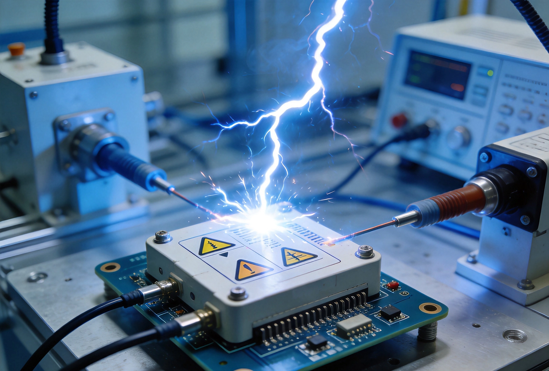
High voltage in PCB context typically means anything above 100 volts AC or DC, though different industries define it differently. Industrial equipment commonly operates at 230V, 400V, 480V, and up to 690V AC in three-phase systems. DC voltages in power conversion can reach similar levels or higher after rectification and boosting.
The critical factor is not just the nominal voltage but the peak transient voltages that occur in real systems. Motor drives and switching power supplies generate voltage spikes that can exceed nominal levels by two to three times during switching events. A 400V nominal system might see 800V peaks, requiring insulation rated for at least that level.
Voltage distribution across the board is rarely uniform. Corners, edges, and points of high curvature concentrate electric fields, making breakdown more likely at these locations. Components that switch high currents, like IGBTs and MOSFETs, generate electromagnetic interference that couples into nearby traces and creates unexpected voltage differences. Designing for high voltage requires accounting for these real-world conditions.
Dielectric strength measures a material's ability to withstand electric field stress without breaking down. It is expressed in volts per mil (V/mil) or kilovolts per millimeter (kV/mm). Higher dielectric strength means the material can withstand higher voltages before experiencing insulation failure.
Standard FR4 typically provides dielectric strength around 500-700 V/mil, or approximately 20-27 kV/mm. However, this value applies to thin samples under controlled conditions. Practical PCB dielectric strength decreases with increasing thickness, time under stress, temperature, and frequency of voltage application. Design engineers should use conservative derating factors when specifying insulation thickness.
Alternative materials offer significantly higher dielectric strength. Polyimide films like Kapton provide 3000-5000 V/mil dielectric strength, making them suitable for extreme high-voltage applications. Ceramic-filled substrates achieve 800-1000 V/mil while maintaining good processability. Specialty materials like PEEK laminates offer 1000-1500 V/mil with excellent Chemical Resistance.
The relationship between dielectric strength and thickness is not linear. Doubling thickness does not double voltage capability because electric fields become non-uniform in thick dielectrics and surface breakdown paths become significant. For high-voltage applications, multiple thinner dielectric layers with air gaps between them often perform better than a single thick layer.
Comparative Tracking Index measures a material's resistance to surface tracking when contaminated with water and exposed to electrical stress. Surface tracking is a conductive carbon path that forms on insulating surfaces when moisture and contaminants combine with voltage to decompose the material. Once tracking initiates, it grows across the surface until it bridges conductors and causes catastrophic failure.
CTI is measured by applying voltage between electrodes on the material surface while dripping ammonium chloride solution between them. The voltage at which tracking initiates determines the CTI rating. Materials are classified into groups based on CTI values: 600V and above is Group I, 400-599V is Group II, 175-399V is Group III, and below 175V is Group IV.
Standard FR4 typically achieves CTI values around 150-200V, placing it in Group III or IV. For industrial environments where moisture and contamination are concerns, materials with CTI above 400V or 600V are preferred. High-CTI materials use different resin chemistries or fillers that resist carbonization during tracking events.
IPC guidelines recommend minimum CTI based on operating voltage and environmental conditions. Higher voltages and harsher environments require higher CTI materials. Some industrial safety standards explicitly require minimum CTI ratings for specific applications. Always verify that your selected material meets CTI requirements for your voltage and environment.
Glass Transition Temperature marks the point where the Pcb Substrate changes from a rigid glassy state to a softer rubbery state. Below Tg, the material maintains its shape and mechanical properties. Above Tg, it becomes more flexible and its thermal expansion increases dramatically. For high-voltage applications where boards may experience elevated temperatures, understanding Tg is essential.
Standard FR4 has Tg around 130-140 degrees Celsius. When operating at temperatures approaching or exceeding Tg, the material's dimensional stability degrades and copper-to-substrate bond strength decreases. In high-voltage applications where partial discharges or surface tracking create localized heating, temperatures can exceed ambient by significant margins.
High-Tg alternatives extend the usable temperature range. Tg 150 materials push the transition temperature higher, while Tg 170 and Tg 180 materials are available for extreme applications. Some manufacturers offer Tg 200+ materials for specialized needs. The trade-off is often cost and processability, as higher Tg typically requires higher lamination temperatures and may be more difficult to machine.
For high-voltage applications, selecting materials with adequate margin between maximum operating temperature and Tg is crucial. A good rule of thumb is maintaining at least 40 degrees Celsius margin between peak operating temperature and Tg. This accounts for hot spots, Thermal Cycling, and temperature measurement uncertainty.
Thermal decomposition temperature indicates when the material begins to chemically break down from thermal stress. This is distinct from Tg, which marks a physical property change. Td specifically measures when the resin matrix starts to decompose, releasing gases and losing mass.
For high-voltage applications, Td matters because partial discharge can create localized temperatures that approach decomposition. Partial discharge occurs when voids or bubbles in the dielectric experience ionization and tiny breakdowns that slowly erode the material. Over thousands of hours, this erosion can penetrate through the insulation and cause complete failure.
Quality High-tg Materials typically have Td values above 300 degrees Celsius. Some specialty materials exceed 350 degrees Celsius. When evaluating materials, ensure that Td significantly exceeds any temperature the board might encounter during fault conditions or sustained operation.
Thermal Conductivity also affects high-voltage reliability. Materials that transfer heat away from hotspots reduce localized temperature rise and extend insulation life. Standard FR4 has relatively low Thermal Conductivity around 0.3 W/mK, while ceramic-filled materials may exceed 1.0 W/mK. For densely packed high-voltage designs, higher thermal conductivity improves reliability.
Surface resistance measures how well the material surface resists electrical current flow. Volume resistivity measures the bulk material resistance. Both properties affect leakage current and insulation performance. High-voltage applications require materials with very high surface and volume resistivity to minimize unwanted current flow.
Standard FR4 provides surface resistance around 10^5 to 10^7 megohms and volume resistivity around 10^6 to 10^8 megohm-centimeters. These values degrade with increasing temperature and humidity. At 85 degrees Celsius and 85% relative humidity, resistance can drop by orders of magnitude.
For high-voltage insulation, materials with resistivity above 10^8 megohms are preferred. Polyimide films offer resistivity above 10^10 megohms, while ceramic substrates may exceed 10^12 megohms. Some specialized materials achieve 10^14-10^16 megohms, though cost and processability become limiting factors.
Surface contamination dramatically reduces effective resistance. Dust, moisture, and ionic contaminants create conductive paths across surfaces. In industrial environments, Conformal Coating over high-voltage circuits provides additional insulation and protects against contamination. The combination of high-resistivity substrate and protective coating achieves the best reliability.
High-voltage PCB construction requires attention to both the laminate material and the prepreg used for multilayer bonding. Prepreg has different properties than laminate due to its partially cured state and different resin content. The combination of materials in a multilayer stack must meet voltage withstand requirements across all layers.
For multilayer high-voltage boards, the dielectric between layers must handle the voltage difference between adjacent conductors. In a power bus structure with 400V between planes, the prepreg must insulate this difference without breakdown or tracking. Thicker prepreg constructions or multiple prepreg layers may be necessary.
Some manufacturers offer high-voltage specific laminate products with enhanced insulation properties. These materials undergo special testing to verify voltage withstand and tracking resistance. Using certified high-voltage materials rather than assuming standard materials will suffice provides documented performance margins.
High-voltage applications sometimes require heavier copper to reduce resistance and handle higher currents alongside the insulation requirements. However, heavy copper affects how the material handles Thermal Cycling and how well plating adheres to the substrate. Standard and heavy Copper Foil treatments differ, potentially affecting dielectric integrity.
Choosing the right foil treatment for high voltage ensures good adhesion without creating stress concentrations that could initiate breakdown. Vlp (very low profile) or Hvlp foil reduces roughness that can concentrate electric fields at the copper-substrate interface. For extreme high-voltage applications, profile measurements and control become important specifications.
Electrical clearance is the shortest path through air between two conductors at different potentials. High-voltage design requires maintaining adequate clearances to prevent arcing across air gaps. Standards like IPC-2221 and IEC 60950 provide clearance tables based on working voltage and pollution degree.
For 400V applications, basic clearance requirements range from approximately 1.5mm to 3mm depending on altitude and pollution degree. Higher voltages require proportionally larger clearances. Designers must also account for transient overvoltages, which may require additional margin beyond steady-state voltage requirements.
Internal clearances within multilayer boards have additional complexity. The voltage difference between adjacent layers drives insulation thickness requirements. If your power planes operate at significantly different voltages, separating them to non-adjacent layers or increasing dielectric thickness may be necessary.
Creepage is the shortest path between two conductors along the surface of the insulating material. Because contaminated surfaces conduct better than air, creepage requirements exceed clearance requirements for the same voltage. This difference is especially pronounced in polluted industrial environments.
Creepage requirements depend on the material's CTI rating. Materials with higher CTI can have shorter creepage distances for equivalent voltage because they resist surface tracking better. Using high-CTI materials effectively reduces board space requirements for high-voltage isolation.
Slots, grooves, and Conformal Coating changes affect creepage paths. Adding a slot between conductors increases the creepage distance by forcing the surface path around the slot. However, the slot also collects contaminants and may not always provide the expected improvement. Design tools that calculate creepage based on your specific geometry help optimize layouts.
Conformal coating provides additional insulation and contamination protection over assembled boards. For high-voltage applications, coating selection significantly affects achievable spacing and reliability. Different coating materials offer different dielectric constants, breakdown strengths, and environmental resistance.
Acrylic conformal coatings provide good general protection with dielectric strength around 900 V/mil. Urethane coatings offer similar protection with better Chemical Resistance. Silicone coatings excel in high-temperature applications but may not provide adequate hardness. Parylene coatings offer exceptional dielectric properties but require specialized application equipment.
Coating thickness matters for high-voltage applications. Standard coating thickness of 25-75 micrometers provides significant additional breakdown protection but may not be adequate for the highest voltage applications. Thick coating or multiple coats may be necessary, with attention to coverage uniformity and any bubbles or voids that could reduce effectiveness.
High-voltage boards should undergo dielectric testing during production to verify insulation integrity. Standard tests include hipot testing, which applies high voltage between conductors and ground to check for breakdown. Test voltage is typically 1.5 to 2 times the maximum working voltage, applied for a specified duration.
Some applications require partial discharge testing that detects tiny breakdowns within the insulation structure. This sensitive test identifies voids, delaminations, or contamination that might not fail hipot testing but could fail in service. Partial discharge testing is more expensive but provides higher confidence for critical applications.
Request test reports and statistical process control data from your manufacturer for high-voltage products. Hipot yield rates, defect rates by type, and trending data indicate process capability. Boards that barely pass hipot testing may have marginal designs that will fail early in field operation.
Industrial high-voltage Pcb Materials cost more than standard FR4. Higher Tg materials, high-CTI formulations, and ceramic fillers all add expense. For cost-sensitive applications, understanding which properties are truly critical enables optimization between cost and reliability.
In many cases, the difference between standard FR4 and mid-range alternatives is modest. A Tg 150 material may cost only 10-20% more than Tg 130 FR4 while providing significantly improved thermal margin. High-CTI materials may cost 30-50% more but enable tighter spacing that reduces board size.
For extreme high-voltage applications, the cost difference becomes more significant. Specialized ceramics and polyimide composites can cost five to ten times more than standard materials. These costs must be justified by the performance requirements and failure cost analysis for your specific application.
Work with your PCB manufacturer early in the Material Selection process. Manufacturers have experience with which material combinations work reliably in their processes and which create challenges. They may have existing qualified materials that meet your requirements, reducing qualification time compared to unfamiliar alternatives.
Provide your manufacturer with voltage, current, and environmental specifications during design. Ask for their recommendations on material selection and whether any of your proposed design features might cause manufacturing or reliability issues. This early collaboration prevents costly redesigns later.
Request material datasheets and verify that the specifications meet your requirements. Pay attention to not just nominal values but also test conditions and sample preparation. A material that looks adequate on datasheet may perform differently in your actual construction and environment.
High-voltage Pcb Material Selection requires balancing multiple electrical, thermal, and mechanical properties. Dielectric strength determines voltage-withstand capability. CTI addresses surface tracking resistance. Tg and Td ensure thermal stability. Resistivity minimizes leakage. Each property affects reliability in different ways.
Standard FR4 may be adequate for some high-voltage applications below 100-200V, but more demanding applications require enhanced materials. Understanding your specific voltage, environment, and reliability requirements enables appropriate material selection without unnecessary cost.
Design for voltage spacing using clearance and creepage requirements from applicable standards. High-CTI materials enable tighter spacing. Conformal coating provides additional protection in harsh environments. Work with your manufacturer to optimize the balance between material performance and design density.
Testing and verification at production and incoming inspection ensure that material selection translates to actual product reliability. Hipot testing, partial discharge testing, and statistical process control data provide confidence in high-voltage insulation integrity.
By carefully evaluating materials against your application requirements, you can achieve reliable high-voltage performance without over-specifying and unnecessarily increasing cost.
Understanding CTE and Its Impact on Industrial PCB Materials SelectionJuly/18/2026
A Comprehensive Guide to High-Tg Materials for Industrial PCBsMay/27/2026
FR-4 vs. Polyimide: Choosing the Right Industrial PCB MaterialsJuly/02/2026
A Comprehensive Guide to High-Tg Materials for Industrial PCBsJune/05/2026
The Rise of Halogen-Free Industrial PCB Materials: Benefits and Trade-offsAugust/06/2026
Copper Weight Matters: Optimizing Industrial PCB Materials for Power ElectronicsSeptember/23/2026
Comparing Isola, Panasonic, and Shengyi: Top Industrial PCB Materials BrandsOctober/19/2026

Panelization Strategies for Efficient Industrial PCB Design and AssemblySeptember/08/2026