Open Nav


Power Electronics demand more from Pcb Materials than their signal-processing counterparts. When your board must deliver hundreds of watts or tens of amps, copper weight becomes a primary design constraint rather than an afterthought. The thickness of copper plating directly determines how much current your traces can carry, how effectively heat transfers from components, and whether your board survives the thermal stresses of real-world operation.
Many engineers specify copper weight without fully understanding the trade-offs involved. Going heavier than necessary increases cost and introduces manufacturing challenges. Going too light creates reliability problems that manifest as field failures, costly repairs, and reputation damage. This guide explains how copper weight interacts with Power Electronics requirements and how to optimize Material Selection for demanding applications.
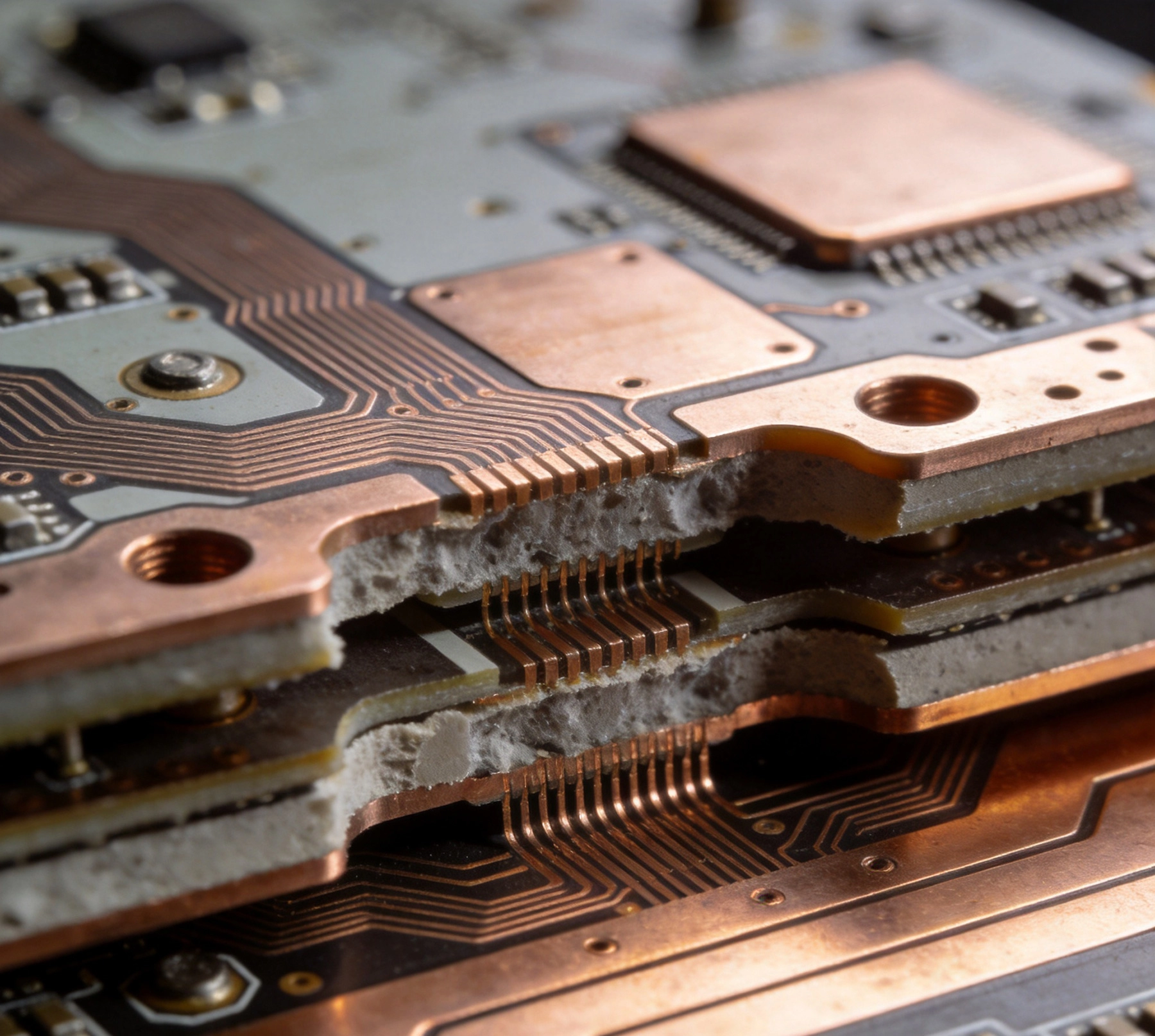
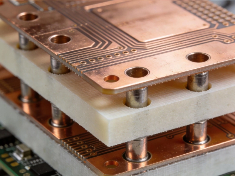
Copper weight describes the mass of copper per unit area, typically expressed in ounces per square foot (oz/ft²). Standard PCB Fabrication uses base copper of 1 oz/ft² (approximately 34 microns or 1.4 mils thickness). When specifications call for heavier copper, manufacturers plate additional copper onto traces and planes to achieve the target weight.
The relationship between weight and thickness is straightforward: 1 oz/ft² equals approximately 34 microns of foil thickness. A 2 oz/ft² specification means approximately 68 microns of copper. These thicker layers enable wider current carrying capacity and improved thermal performance but require modified manufacturing processes.
Standard PCB processes handle copper weights up to about 2 oz/ft² routinely. Beyond this, heavy copper processes apply additional plating steps to achieve specified weights. Common heavy copper specifications range from 3 oz/ft² to 10 oz/ft², with some extreme applications requiring even thicker plating.
Heavy copper Pcb Manufacturing differs from standard processing in several ways. Etching compensation must account for non-uniform etch rates on Thick Copper. Plating processes must achieve consistent coverage across large areas. Lamination parameters may need adjustment to prevent foil distortion. These differences add cost and require manufacturers with specific heavy copper experience.
Electrical current flowing through a conductor generates heat according to the power dissipation equation (I²R). Higher current produces more heat, and higher resistance produces more heat for a given current. Trace resistance depends on trace geometry (width, length, and thickness) and copper resistivity. Doubling copper thickness halves the trace resistance, reducing heat generation by half for the same current.
This relationship explains why heavy copper dramatically improves current carrying capacity. A trace with 3 oz/ft² copper carries significantly more current than the same width trace with 1 oz/ft². The exact relationship involves thermal considerations, as the heat generated must dissipate somehow.
Current carrying capacity is ultimately limited by acceptable temperature rise. Current flowing through trace resistance generates heat that must flow to the surrounding environment. If heat generation exceeds Heat Dissipation, temperature rises until equilibrium is reached at some acceptable level. Pcb Design standards like IPC-2152 provide guidance on current capacity based on temperature rise assumptions.
Temperature rise limits depend on application requirements. Consumer electronics may tolerate 20-30°C rise above ambient. Industrial equipment often requires limiting rise to 10-20°C. High-reliability applications may specify even tighter limits. Your temperature rise requirement directly affects trace width calculations and thus Copper Weight Selection.
For a given current and acceptable temperature rise, trace width depends on copper thickness. Standard IPC formulas and calculators incorporate copper weight into width calculations. Using heavier copper allows narrower traces for the same current, potentially enabling significant board space savings. However, the benefit diminishes at some point as other factors limit practical trace widths.
Practical trace width calculations should use appropriate safety margins. IPC-2152 charts provide baseline guidance, but field experience often justifies additional margin for challenging environments. Consult with your manufacturer about their process capabilities and any adjustments recommended for your specific conditions.
Copper conducts heat as well as electricity, with Thermal Conductivity approximately 400 W/m·K. This high conductivity makes copper planes effective heat spreaders, distributing thermal energy from concentrated heat sources across larger areas. Heavy copper planes spread heat more effectively than thin copper, reducing local temperature peaks.
Power plane design for Thermal Management requires careful attention to how heat flows from components to the plane and from the plane to the environment. Thermal Vias transfer heat from component pads to internal planes, where copper spreads the heat before it reaches board edges or surface air. Heavier copper improves this spreading effect.
Thermal Vias connect component pads to copper planes, providing low-resistance thermal paths. The effectiveness of thermal vias depends on their number, size, and plating thickness. Heavier copper plating on via barrels improves Thermal Conductivity proportionally. A via plated to 2 oz/ft² carries significantly more heat than the same size via with standard plating.
Thermal via array design balances thermal performance against manufacturing constraints and component density. More vias provide better thermal paths but may conflict with routing needs or component pads. The thermal conductivity of the via barrel copper often limits heat transfer more than via geometry.
Power components like MOSFETs, voltage regulators, and motor drivers generate significant heat that must reach the PCB for dissipation. The thermal path from component junction through package, solder joint, pad, plane, and finally to ambient involves multiple thermal resistances. Copper weight affects the resistance of the solder joint and pad portion of this path.
Heavy copper on thermal pads improves heat transfer from components to the PCB plane. This improvement often enables higher power dissipation without additional heat sinks or active cooling. The cost of heavy copper may be less than the cost of adding external cooling solutions.
Copper Weight Selection interacts with laminate material properties. The substrate material provides mechanical support and electrical isolation, but its thermal conductivity is far lower than copper (typically 0.3-0.5 W/m·K for FR4). This thermal mismatch means heat spreads primarily through copper planes rather than through the laminate.
Laminate selection for power electronics considers thermal conductivity, Glass Transition Temperature (Tg), and thermal decomposition temperature (Td). Higher Tg materials maintain mechanical integrity at elevated temperatures, important when power dissipation raises board temperatures. Some laminate formulations offer enhanced thermal conductivity for power applications.
Standard FR4 has thermal conductivity around 0.3 W/m·K, which limits heat flow through the board thickness. Metal core substrates (IMS) place a thermal conductive aluminum or copper layer between the circuit layers and a dielectric. This construction dramatically improves thermal transfer from components to the metal core, where heat spreads efficiently to heat sinks or ambient air.
Metal core PCBs cost more than standard boards but may provide the only viable thermal solution for high-power components. Evaluate whether your power levels justify metal core construction or whether heavy copper on standard substrate provides adequate thermal performance.
Power electronics operating in demanding environments benefit from laminate materials with elevated thermal ratings. High-Tg FR4 (typically 150°C or higher) maintains mechanical stability at temperatures that would soften standard materials. This stability matters when Thermal Cycling stresses board construction and solder joints.
For the most demanding applications, polyimide and other high-performance materials offer superior thermal resistance. These materials cost more but survive conditions that would degrade standard FR4. Consider Material Selection as part of the overall optimization for your application environment.
Heavy copper PCBs require modified manufacturing processes that not all manufacturers handle well. The additional plating steps needed for Thick Copper introduce opportunities for variation and defect. Ask potential manufacturers about their heavy copper experience and quality track record.
Etching behavior changes with heavy copper. Sidewall angle becomes shallower, affecting impedance characteristics. Trace width control becomes more challenging. These factors require compensation in design data and process control adjustments.
Uniform plating across large panels requires careful process control. Non-uniform plating creates local thickness variations that affect current capacity and impedance. Ask about plating thickness specifications and how manufacturers verify uniformity.
Minimum plating thickness specifications should be met or exceeded across the usable board area. Some manufacturers specify average thickness while others specify minimum values. Understand what guarantees apply to your order.
Heavy copper affects registration tolerances between layers. Thicker copper means deeper etching, potentially affecting annular ring tolerances. Ask about layer-to-layer registration capability for heavy copper designs and whether any design rule adjustments are needed.
Via formation also changes with heavy copper. Larger drills create larger holes, and plating thickness relative to hole size affects aspect ratio. Manufacturers with heavy copper experience understand these interactions and can advise on achievable tolerances.
Not all traces on a power board need heavy copper. Signal traces carrying milliamps can use standard copper weight while power traces carry amps. Selective heavy copper applies thick plating only where needed, optimizing cost while achieving required current capacity. This approach requires careful coordination between design intent and manufacturing capability.
Selective heavy copper typically costs more than uniform heavy copper due to additional process steps, but may still cost less than full heavy copper when power sections represent only part of the board. Evaluate the cost tradeoff for your specific design.
When heavy copper alone cannot achieve required current capacity, parallel traces distribute current across multiple conductors. This approach requires careful layout to ensure balanced current sharing, but provides flexibility beyond single-trace limitations.
Split planes can similarly distribute current across multiple plane segments. This technique also provides flexibility in routing and Thermal Management but requires attention to current return paths and ground integrity.
Extremely high current applications may require external bus bars in addition to PCB copper. Bus bars are separate metal conductors that bolt or solder to PCB pads, providing current capacity beyond what reasonable trace widths can achieve. This approach separates high-current and signal routing concerns.
Bus bar design requires mechanical consideration of mounting and thermal expansion. The connection between bus bar and PCB must handle both electrical current and mechanical stress. These details require careful engineering attention.
Motor drive applications typically involve high currents at moderate voltages. Phase outputs carrying tens of amps require careful copper sizing. Gate drive circuits with fast transitions benefit from Controlled Impedance traces despite relatively low current levels, separating impedance requirements from power requirements.
Motor drive Pcb Design often combines heavy copper for power sections with Controlled Impedance for gate drives. This mixed approach requires stack-up planning that accommodates both requirements. Some designs use dedicated layers for each function.
Switching power supplies involve high-frequency currents that create skin effect and proximity effect losses. While skin effect is negligible at typical switching frequencies for standard copper thickness, proximity effects in multilayer transformers can increase effective resistance. Heavy copper may not improve performance and could worsen proximity losses in tightly coupled windings.
Consult with power supply specialists when designing high-frequency power stages. The interactions between trace geometry, layer assignment, and switching frequency require expertise beyond basic current capacity calculations.
Battery management systems must handle high charge and discharge currents while maintaining precise voltage sensing. Current sensing traces require careful layout to avoid measurement errors from IR drops. Heavy copper sense traces minimize IR drop but also reduce the voltage being measured.
Kelvin connections for sensing separate current-carrying and voltage-sensing paths, eliminating measurement errors from trace resistance. This technique is essential for accurate state-of-charge estimation in high-current battery systems.
High-power LED drivers must dissipate heat while maintaining tight current regulation. LED thermal management often limits maximum drive current, making effective heat spreading critical for maximizing light output. Heavy copper planes provide effective thermal spreading from LED mounting pads.
LED driver designs also involve switching regulators with high-frequency considerations. Balance thermal management for power components with appropriate impedance control for switching nodes. Mixed approaches often yield optimal results.
Heavy Copper Pcb costs exceed standard PCB costs due to additional processing steps and lower manufacturing throughput. Cost factors include plating time, process yield effects, and tooling adjustments. The premium varies by manufacturer and by specific weight requirements.
Evaluate whether heavy copper costs align with performance benefits. In some cases, external heat sinks, fans, or liquid cooling may cost less than heavy copper for the same thermal improvement. In others, heavy copper provides the only viable solution within product form factor constraints.
Work with manufacturers early in design to understand their heavy copper capabilities and cost structure. Some weights may represent capability limits where cost jumps significantly. Designing to manufacturable weights avoids unnecessary cost premiums.
Panel utilization affects Heavy Copper Pcb pricing as it does standard boards. Maximize utilization to reduce per-board costs. Some designs may benefit from panelization strategies that improve yield and throughput.
Use IPC-2152 charts or calculators as starting points for trace width calculations. Input your current requirement, acceptable temperature rise, copper weight, and trace length. Add appropriate safety margins for your application environment and reliability requirements. For critical applications, testing validates calculations under actual conditions.
Practical maximum copper weight depends on manufacturer capability and design complexity. Many manufacturers routinely handle up to 10 oz/ft². Extreme weights like 20 oz/ft² or higher require specialized processing and limited manufacturers. Discuss specific requirements with potential manufacturers early.
Heavier copper affects trace geometry and thus impedance. Thicker copper with the same width produces lower impedance, and sidewall angle changes affect characteristic impedance. Work with your manufacturer to characterize impedance for heavy copper designs. You may need to adjust trace widths to hit impedance targets.
Heavy copper planes and pads dissipate heat differently than standard copper during soldering. Larger thermal mass requires longer dwell times at soldering temperature. Assembly processes may need adjustment for heavy copper boards. Discuss assembly considerations with your manufacturer.
Yes, different layers can have different copper weights in the same board. This approach optimizes cost by applying heavy copper only where needed. However, layer weight differences complicate lamination and may affect flatness. Discuss mixed-weight requirements with manufacturers to verify they can handle the construction.
Copper weight selection for power electronics requires balancing current capacity, thermal management, manufacturing capability, and cost. The right copper weight depends on your specific current levels, acceptable temperature rise, and application environment. Optimize by starting with calculations, verifying with manufacturer input, and testing under realistic conditions.
Heavy copper provides substantial benefits for power electronics but requires appropriate manufacturing partners and design practices. Invest time in understanding manufacturer capabilities and designing to achievable specifications. The performance improvements from proper copper weight selection often justify the additional complexity.
A Comprehensive Guide to High-Tg Materials for Industrial PCBsJune/05/2026
How to Select Industrial PCB Materials for High-Voltage ApplicationsSeptember/07/2026
The Rise of Halogen-Free Industrial PCB Materials: Benefits and Trade-offsAugust/06/2026
A Comprehensive Guide to High-Tg Materials for Industrial PCBsMay/27/2026
Understanding CTE and Its Impact on Industrial PCB Materials SelectionJuly/18/2026
FR-4 vs. Polyimide: Choosing the Right Industrial PCB MaterialsJuly/02/2026
Innovative Industrial PCB Solutions for Renewable Energy SystemsAugust/10/2026
Materials, Methods, and Industry Standards ExplainedMay/27/2026