Open Nav


Industrial Power Electronics, EV charging systems, motor drives, and high-current distribution boards increasingly require copper weights far beyond the standard 1oz or 2oz. When copper thickness reaches 10oz (approximately 350μm) or higher, conventional Pcb Manufacturing methods are no longer sufficient. Achieving 10oz+ copper reliably depends less on simply "adding more copper" and more on selecting the right combination of plating, lamination, etching, and process control techniques.
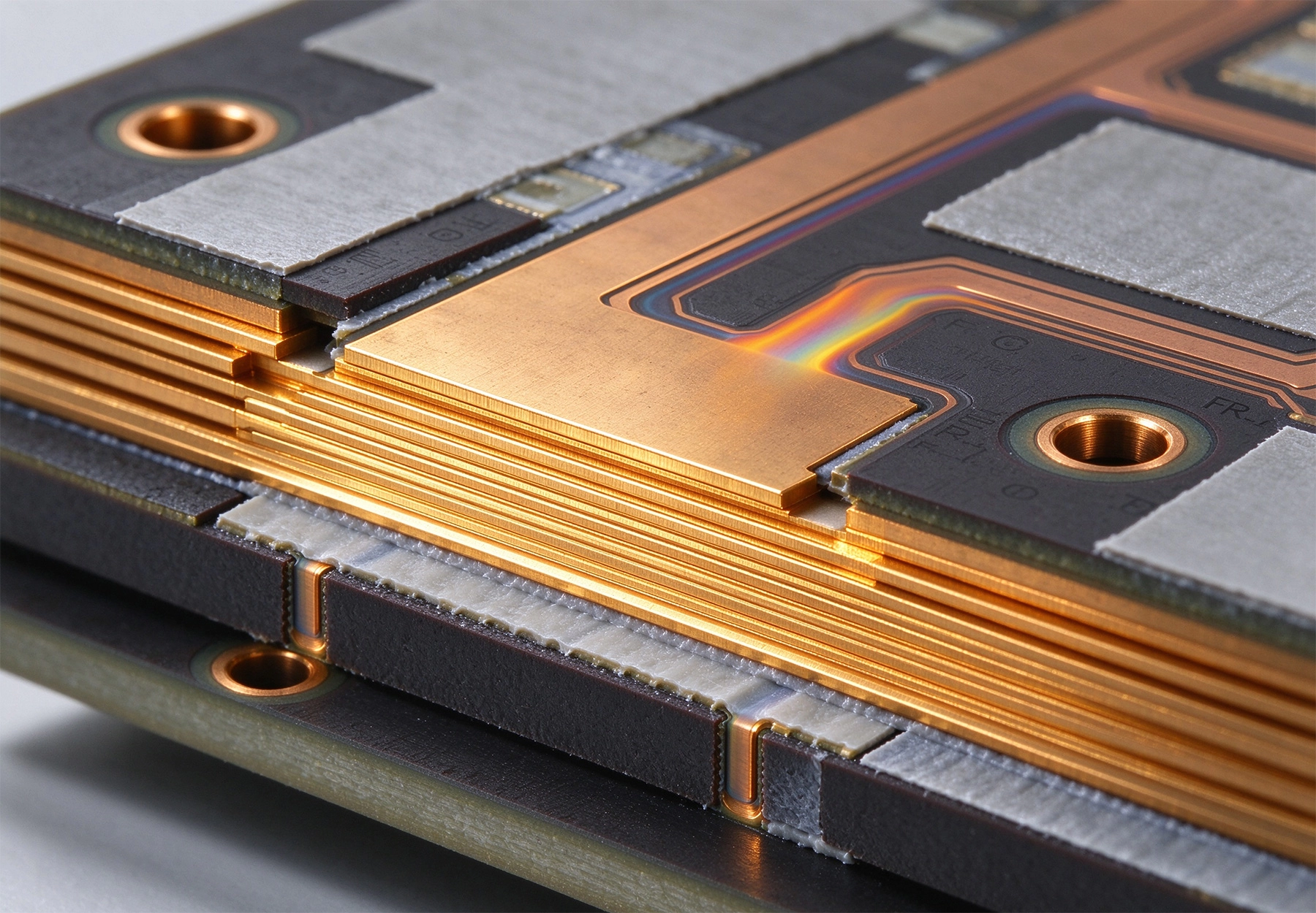
Standard PCBs typically use 0.5oz to 2oz copper. Heavy copper boards are generally defined as 3oz or above, while 10oz and beyond are considered ultra-heavy copper. At this thickness, the main challenges shift from basic conductivity to manufacturing control:
For these reasons, 10oz+ copper is not produced by extending a standard plating cycle. It requires a structured build-up strategy.
The most direct way to achieve very Thick Copper is to start with heavy copper-clad laminates. Instead of building all copper thickness through plating, manufacturers laminate Thick Copper foil onto the substrate under controlled heat and pressure. This method provides a solid base layer and reduces the amount of copper that must be deposited electrochemically.
For multilayer boards, thick copper foils are combined with prepreg materials that have sufficient resin flow to fill the deep gaps between heavy traces. Without adequate resin flow, voids and Delamination risks increase significantly.
Electroplating remains the core technique for increasing copper thickness beyond the initial foil weight. In acid copper plating, the PCB acts as the cathode while copper anodes dissolve into the bath. Copper ions deposit onto exposed conductive surfaces, gradually increasing thickness.
For 10oz+ boards, plating must be carefully controlled. Typical process parameters include copper concentration around 60–80 g/L, sulfuric acid around 180–220 g/L, temperature between 20–28°C, and current density adjusted to balance deposition rate with uniformity. Longer plating times are required, but simply plating longer without process control leads to rough deposits, edge overbuild, and poor through-hole coverage.
Step plating, also called differential plating, is one of the most important techniques for ultra-heavy copper. Instead of trying to reach 10oz+ in a single operation, copper is built up through multiple plating cycles. Each cycle adds a controlled thickness, allowing manufacturers to manage stress, uniformity, and surface quality more effectively.
This approach is especially useful when different areas of the board require different copper weights. For example, power traces may need 10oz while signal areas remain at 2oz or 3oz. Step plating enables selective thickening without over-plating the entire board.
Pulse plating applies current in controlled pulses rather than continuous direct current. Reverse-pulse plating alternates between forward deposition and brief reverse cycles. These techniques improve throwing power, reduce internal stress, and help achieve more uniform copper distribution in deep features and high-aspect-ratio holes.
For 10oz+ PCBs, pulse plating can reduce thickness variation between board edges and centers. It also helps prevent brittle deposits that may crack during Thermal Cycling or mechanical stress.
In pattern plating, photoresist defines where copper will be deposited. Copper is then plated only on exposed conductive areas, including traces, pads, and via barrels. After plating, the resist is stripped and the remaining base copper is etched away.
For ultra-heavy copper, pattern plating is often combined with differential etching. This reduces the amount of copper that must be removed chemically, limiting undercut and improving sidewall definition. The result is straighter trace profiles compared with etching a fully laminated 10oz foil from the start.
Before heavy plating begins, the copper surface must be clean, active, and free of oxidation or organic contamination. Alkaline degreasing, micro-etching, and acid activation help ensure strong adhesion between the base copper and the plated layer. Poor pre-treatment can cause voids, peeling, or uneven deposition, especially after long plating cycles.
Acid copper baths rely on accelerators, suppressors, and levelers to control deposition behavior. Accelerators promote fine-grain deposition, suppressors prevent excessive buildup at high-current-density areas, and levelers improve surface flatness. For 10oz+ plating, additive balance becomes more critical because small deviations are amplified over long deposition times.
Uniform copper deposition requires consistent ion supply across the board surface. Air agitation, mechanical movement, and bath circulation help prevent depletion zones where copper ions are consumed faster than they can be replenished. Without adequate agitation, thick plating may develop roughness, nodules, or localized thin spots.
Very thick copper layers store significant internal stress. If plating is too fast or additives are unbalanced, the deposit may become brittle. Manufacturers may use intermediate baking, stress-relief steps, or controlled current profiles to reduce cracking risk. This is especially important for boards that will experience repeated Thermal Cycling in industrial environments.
In 10oz+ PCBs, vias must carry high current and survive mechanical and thermal stress. Standard via plating thickness is often insufficient for ultra-heavy copper applications. Manufacturers typically increase via barrel copper and pay special attention to annular ring design.
Large-diameter vias, copper-filled vias, or plated-through slots are commonly used to improve current transfer and Heat Dissipation. Because thick outer copper increases the effective hole aspect ratio, drilling, desmear, and activation steps must be tightly controlled to avoid voids or poor wall coverage.
Plating alone does not complete a 10oz+ PCB. Once the required copper thickness is achieved, unwanted copper must be removed to form traces. Thick copper etching is more difficult than standard etching because side etching becomes more pronounced. If not controlled, traces can develop tapered or mushroom-shaped profiles, reducing effective cross-sectional area and current capacity.
To manage this, manufacturers may use multi-stage etching, low-undercut etchants, laser direct imaging for accurate pattern definition, and differential etching strategies that minimize the amount of copper removed in a single step.
Standard screen-printed Solder Mask often performs poorly on 10oz+ boards. The deep valleys between tall copper traces can cause ink pooling, while trace tops may receive insufficient coverage. Electrostatic spray Solder Mask is frequently preferred because it provides more uniform thickness over uneven copper topography.
Surface finish selection must also account for assembly conditions. Thick copper absorbs more heat during reflow, so solder profiles may need adjustment. Common finishes include ENIG, immersion silver, HASL, and OSP, depending on reliability, solderability, and environmental requirements.
Producing 10oz+ copper PCBs successfully requires early collaboration between design and fabrication teams. Key inputs include target copper weight, current requirements, via structure, trace width and spacing, layer stackup, and acceptable tolerances. Because ultra-heavy copper processes vary between manufacturers, design rules should be confirmed before finalizing the layout.
Specifying copper weight clearly in fabrication notes helps avoid misinterpretation. For example, a requirement such as "10oz outer layer after plating" should distinguish between base foil thickness and final plated thickness.
Achieving 10oz+ copper in industrial PCBs requires more than extended plating time. The most reliable results come from combining heavy Copper Foil lamination, controlled electroplating, step or differential plating, pulse plating where appropriate, and carefully managed etching. Supporting processes such as pre-treatment, additive control, agitation, stress management, via plating, and solder mask application all influence final quality.
For high-current industrial applications, 10oz+ copper improves current capacity, reduces resistive losses, and enhances thermal performance. However, it also increases manufacturing complexity. Selecting a fabricator with proven ultra-heavy copper capability and involving them early in the design phase are essential steps for achieving consistent, high-reliability results.
It is possible in some cases, but most manufacturers combine heavy Copper Foil lamination with electroplating. Pure plating build-up to 10oz+ requires very long cycles and tight process control, so hybrid approaches are more practical.
Standard plating deposits copper in a continuous operation. Step plating builds copper thickness through multiple controlled cycles, allowing better management of uniformity, stress, and selective thickening.
Pulse and reverse-pulse plating improve throwing power, reduce internal stress, and help produce more uniform deposits. This is valuable when plating thick copper on large boards or into deep vias.
Yes. Thick copper creates large height differences between traces and substrate. Electrostatic spray solder mask is often preferred over screen printing because it provides more uniform coverage.
Typical applications include EV charging stations, industrial motor controllers, power converters, inverters, welding equipment, battery management systems, and high-Power Distribution assemblies.
How to Prevent Electrochemical Migration (CAF) for Better Industrial PCB ReliabilitySeptember/04/2026
The Role of Conformal Coating in Enhancing Industrial PCB ReliabilityJuly/17/2026
How to Enhance the Mechanical Strength of HDI StructuresSeptember/07/2026
Vibration and Shock: Designing for Industrial PCB Reliability in AutomationJune/30/2026
Ensuring Industrial PCB Reliability in Extreme Environmental ConditionsMay/27/2026
Thermal Management Strategies for Long-Term Industrial PCB ReliabilityJune/04/2026
Top 5 Causes of Failure and How to Improve Industrial PCB ReliabilitySeptember/21/2026
Managing Moisture Sensitivity Levels (MSL) in Industrial PCBAOctober/22/2026