Open Nav


Reducing costs in high-volume Industrial Pcb production is not about cutting corners — it is about eliminating waste, optimizing Design For Manufacturing efficiency, and making strategic decisions at every stage of the product lifecycle. The factories and engineering teams that consistently achieve the lowest total cost of production are not simply accepting the lowest quoted price from their manufacturer. They are actively engineering cost out of the product and the process through deliberate, systematic effort.
For engineers and procurement teams working with contract manufacturers in China, understanding where production costs come from — and where they can be reduced without sacrificing quality or reliability — is a skill that compounds significantly over time and across product volumes. This article examines the most impactful cost reduction strategies across design, component sourcing, manufacturing process, and Supply Chain Management.
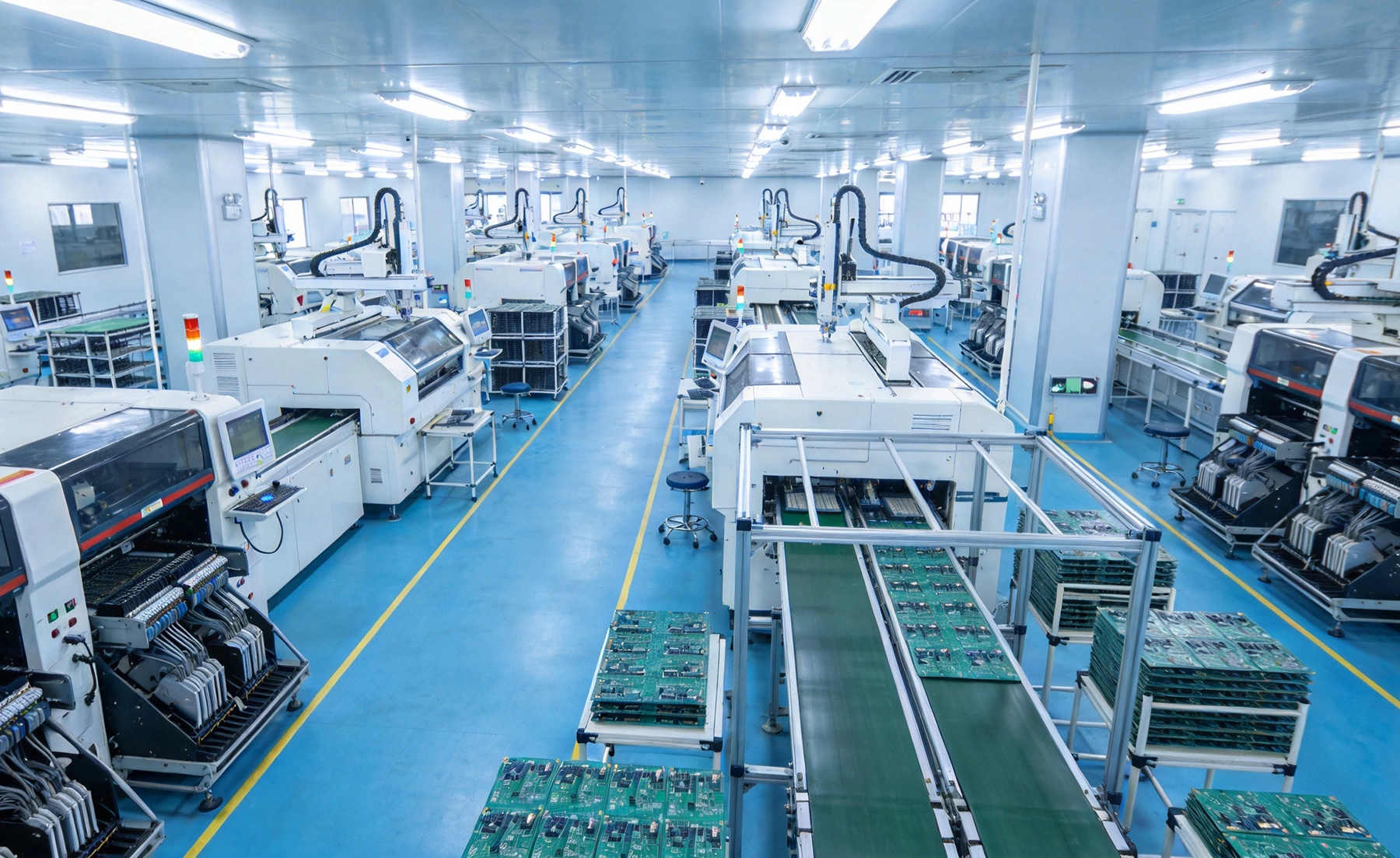
No other cost reduction strategy comes close to the impact of Design For Manufacturability. A board that is designed well for the production process costs less to manufacture at every stage — assembly, inspection, testing, and shipment. A board that is designed poorly incurs extra cost at every one of those same stages. The difference in total cost between a DFM-optimized design and a DFM-naive design can exceed 30% in some cases, dwarfing any savings achievable through negotiation or volume purchasing alone.
PCB panels are manufactured in standard sheet sizes — commonly 18x24 inches, 21x24 inches, or 22x26 inches in Chinese fabs. The number of boards that fit into a single panel directly affects the cost per board: more boards per panel means the fixed cost of the panel — lamination, drilling, plating, and tooling — is spread over more units.
Optimizing panel utilization means designing the board dimensions to maximize the quantity fitting on a standard panel, and designing the panelization layout to minimize waste. For example, a board that is 120mm x 80mm can fit 36 units on an 18x24 panel with minimal waste. The same board at 125mm x 82mm might fit only 30 units — a 17% reduction in utilization for a 4% change in dimensions.
Beyond the board outline itself, the panelization approach matters. Arrays with tooling strips on all four sides maximize usable area. V-scoring between boards is cheaper than tab-routing but requires sufficient clearance between the V-groove and the board edge. Mouse bites require additional material and labor but allow for more complex array shapes. The right approach depends on the board geometry and the manufacturer's capabilities.
Every additional layer in a PCB adds cost — more material, more lamination cycles, more drill time, more tooling complexity. A board that requires 6 layers may have been designed with 6 layers because of electrical requirements, but in many cases, a board can be reduced from 6 to 4 layers through smarter distribution of power and ground planes or better use of internal routing. Each layer reduction typically saves 15–25% on the board fabrication cost.
The layer stackup itself also affects cost. Standard High-tg Fr-4 is cheaper than specialty materials. Building the board with fewer unique dielectric thicknesses is cheaper than many thin-ply buildup layers. Communicating your performance requirements clearly — and challenging whether each specification is truly necessary — often reveals opportunities to use lower-cost materials without sacrificing the performance that actually matters.
Tighter tolerances cost money. A Controlled Impedance trace that must be held to ±10% impedance tolerance requires more fabrication process control than one at ±15%. A Blind Via costs significantly more than a through-hole via. A minimum trace width of 4 mil costs more to produce reliably than 5 mil. A slot machined to ±0.1mm tolerance requires more expensive tooling than one toleranced at ±0.2mm.
The principle here is not to loosen every tolerance indiscriminately — critical performance features should be held to the tolerances they require. But in non-critical areas, using the loosest tolerance the design actually requires avoids paying for precision that adds no value. A thorough DFM review with the manufacturer identifies where cost can be saved without risk.
Via costs vary significantly by type and size. Standard through-hole vias are the cheapest. Blind Vias — which connect only some layers — are more expensive. Buried vias — which connect internal layers only — are the most expensive. In a typical multilayer board, the mix of via types and sizes can represent 10–20% of the total board cost.
Reducing via costs means using the simplest via type that meets the electrical requirement. For example, a design that uses blind and buried vias to reduce layer count might actually cost more than a simpler design with more layers and only through-hole vias. Via aspect ratio — the ratio of board thickness to drill diameter — also affects cost significantly. A board that is 3.2mm thick with 0.3mm vias has an aspect ratio of about 10:1, which most standard fab processes can handle without special treatment. Going to 0.2mm vias in the same board increases complexity and cost.
Every unique component in a BOM adds cost — it must be procured, stocked, loaded onto a feeder, and accounted for in quality records. A board that uses 85 different component part numbers costs significantly more to assemble than one that uses 50 — even if the total component cost is similar — because the per-unit handling, setup, and management overhead scales with the number of unique parts.
Part standardization opportunities exist in most designs:
Design teams that maintain preferred parts lists aligned with their contract manufacturer's stock significantly reduce component sourcing costs. When the manufacturer's procurement team can pull components from existing inventory rather than placing new purchase orders, the cost is lower and the lead time is shorter. Negotiating a preferred parts agreement — where both the customer and the manufacturer commit to using a defined set of components for new designs — creates a virtuous cycle where both parties benefit from volume purchasing.
Component pricing is highly volume-dependent, particularly for semiconductors. A standard microcontroller that costs $3.20 per unit at 1,000-unit annual volume might be available at $1.80 per unit at 100,000 units — a 44% reduction from volume alone. Securing long-term pricing agreements with distributors or franchise relationships with manufacturers can lock in favorable pricing for 12–24 months, protecting against price increases and enabling accurate product costing for longer sales cycles.
Single-source components represent both a cost risk and a supply risk. When a sole-source component is the only option for a particular function, the supplier controls pricing. Qualification of alternate sources — even for a limited set of critical components — creates competitive pressure that keeps pricing favorable and protects against supply disruptions that could halt production.
The key is to identify second sources early, not after a primary supplier raises prices or goes on allocation. Validating a second source during stable supply conditions takes weeks; trying to qualify a backup during a supply crisis takes months and costs far more in rush premiums and expedited shipping.
The solder paste stencil is a low-cost consumable with a disproportionate impact on assembly quality and yield. A laser-cut stainless steel stencil with electropolished walls costs slightly more than a chemically etched stencil but delivers significantly better paste release — particularly for fine-pitch components. The improved release translates to higher first-pass yield and lower rework cost, typically paying for the stencil premium within the first few thousand boards.
Stencil aperture design is equally important. Apertures that are correctly sized for the pad geometry — neither too large (causing bridges) nor too small (causing insufficient solder) — maximize first-pass yield. Nano-coating on stencils reduces paste adhesion to the stencil walls, further improving release and reducing the frequency of stencil cleaning during production runs.
In high-volume production, every minute of line downtime costs money. Changeover time — the period when the line is stopped while operators load new components for a different board variant — is pure non-productive time. Optimizing feeder setups to minimize changeover is a well-established discipline in contract manufacturing.
Strategies include designing products to share common component sizes across the product range (so the same feeder types can be reused), pre-loading feeders for the next production run while the current run is in progress, and using quick-change feeder systems that reduce the mechanical setup time per feeder. A line that reduces changeover time from 45 minutes to 15 minutes per run effectively increases productive capacity by the equivalent of running additional boards during that recovered time.
Running multiple identical boards in a single assembly pass — called multi-up assembly — amortizes the fixed setup time of each production run across more boards. A panel that holds four boards requires the same stencil, feeder setup, and reflow profile as a single board, but produces four times as many finished units. For high-volume products where the board fits, multi-up assembly is one of the most effective ways to reduce per-unit assembly cost.
A well-optimized reflow profile minimizes cycle time without compromising solder joint quality. A shorter reflow profile means the oven processes more boards per hour. Optimization typically involves finding the minimum soak time and peak temperature that produces acceptable solder joints across all component types on the board — particularly components with large thermal mass that heat more slowly than small components. Nitrogen atmosphere in the reflow zone reduces oxidation and can allow lower peak temperatures, but the cost of nitrogen must be weighed against the savings from faster cycle times and reduced defect rates.
Many design teams specify board parameters that exceed their actual requirements — sometimes because they copied specifications from a previous design, sometimes because they lack familiarity with what the manufacturing process can deliver. Communicating with the fab about what you actually need — and accepting their recommendations for standard specifications where they are adequate — often yields significant savings.
Standard FR-4 (Tg 130°C) is less expensive than high-Tg alternatives. Standard Solder Mask colors (green) are less expensive than specialty colors (red, blue, white) due to volume and availability. ENIG surface finish is a standard, well-understood process that most fabs can produce efficiently. HASL is less expensive than ENIG but less flat — the right choice depends on the board's actual requirements, not on habit or convention.
PCB fabricators price jobs partly based on how efficiently they fit into their production workflow. Jobs that require non-standard panel sizes or special tooling setups that interrupt the normal production flow carry a pricing premium. Designing boards to fit standard panel sizes used by your manufacturer — and specifying common stackup configurations that match their standard process — reduces the fab's setup cost and is typically reflected in better pricing.
PCB fabricators have capacity and pricing that varies by technology type. Standard through-hole multilayer boards are produced on one set of equipment; high-density interconnect (HDI) boards with laser-drilled Microvias are produced on different, more expensive equipment. Using HDI features — Microvias, 50-micron traces — when standard technology would suffice adds cost without benefit. Challenging each advanced technology requirement and reserving HDI for the sections of the board that genuinely require it is a consistent source of cost savings in multilayer board fabrication.
When the contract manufacturer procures components on your behalf — turnkey manufacturing — they combine procurement across multiple customers and benefit from volume pricing, warehouse the components, and manage the supply chain. This approach is typically more cost-effective than consignment (where you procure components and ship them to the factory) for several reasons: manufacturers have established relationships with major distributors, they buy in volumes that qualify for better pricing, and they absorb the cost of inventory carrying and shortage management.
The trade-off is less visibility and control over component sourcing. For components with specific traceability requirements or for designs that use expensive components where you want visibility into unit costs, consignment or partial consignment may be preferable. The right model depends on the product, the volume, and the relationship with the manufacturer.
For production in China with shipment to North America, Europe, or other destinations, logistics costs can represent 3–8% of the total product cost. Optimizing logistics means consolidating shipments to reduce per-unit freight costs, using freight modes appropriate to the lead time requirement (ocean freight for standard delivery, air freight only for genuine emergencies), and working with manufacturers who have established relationships with freight forwarders and can negotiate better rates than an individual buyer.
Using a freight forwarder that specializes in electronics and has experience with customs documentation, import duty classification, and compliance requirements prevents costly delays and unexpected duty assessments that inflate the landed cost of boards.
Expedited production and shipping are among the most expensive options in Pcb Manufacturing. A standard lead time of 2–3 weeks for board fabrication and 1–2 weeks for assembly is dramatically less expensive than the same order rushed to 5–7 days. For high-volume products with predictable demand, planning production runs to match standard lead times rather than relying on expedited schedules is a reliable way to reduce cost.
Many manufacturers offer pricing incentives for committed long-term capacity — guaranteeing a certain number of board placements or square footage per month in exchange for pricing concessions. If your volume is predictable and steady, these arrangements typically benefit both parties: the manufacturer gets production visibility and the customer gets lower pricing and preferred scheduling.
Counterintuitively, investing in quality is one of the most effective cost reduction strategies available. A factory with 95% first-pass yield produces boards at a significantly lower effective cost than one with 85% yield, because every board that fails first-pass test must be reworked or scrapped — adding labor, material, and delay costs that do not appear in the initial quoted price.
The factories that achieve the highest first-pass yields share common characteristics: rigorous incoming inspection of components, automated in-process inspection (SPI, Aoi, X-ray) at multiple stages, well-maintained equipment with regular calibration, and a culture of treating defects as engineering problems to be solved rather than acceptable byproducts of manufacturing.
When evaluating contract manufacturers, asking about first-pass yield rates — and verifying the data through production samples and pilot runs — is one of the most direct ways to assess the true cost of manufacturing, not just the quoted price.
Cost reduction in high-volume Industrial Pcb production is a multi-dimensional discipline that rewards systematic effort rather than one-time actions. The most impactful strategies — DFM optimization, panel utilization, component standardization, and quality investment — require engineering effort and collaboration with the manufacturer, but they deliver compounding returns that build over successive product generations.
The lowest total cost of production is rarely achieved by simply finding the cheapest manufacturer or negotiating the lowest quoted price. It is achieved by engineering cost out of the product, optimizing the supply chain, and building a collaborative relationship with a manufacturing partner who has the capability and incentive to identify cost reduction opportunities as they arise.
For teams sourcing from Chinese manufacturers, the factories that deliver the best long-term value are typically those that engage early in the design phase, offer substantive DFM recommendations, and share quality and yield data transparently. That level of partnership, built over time, is what makes cost reduction a continuous activity rather than a one-time negotiation.
Design For Manufacturability optimization delivers the largest and most sustainable cost reductions. Designing board dimensions to maximize panel utilization, minimizing layer count and via complexity, specifying the loosest tolerances that meet actual performance requirements, and standardizing component packages all reduce manufacturing cost without sacrificing quality. These design decisions compound across high volumes — a 10% reduction in material cost or assembly time per board translates directly to tens or hundreds of thousands of dollars in savings at high volume.
Panel utilization measures how much of a standard manufacturing panel is occupied by your boards. Higher utilization means the fixed cost of each panel — lamination, drilling, plating — is spread across more boards, reducing the per-board cost. Optimizing board dimensions to fit more units per panel and choosing the right panelization method (V-score, tab-route, or mouse bite) can reduce per-board fabrication cost by 15–25% compared to a poorly utilized layout. This optimization is purely a design exercise with no impact on board performance.
In turnkey manufacturing, the contract manufacturer procures all components on your behalf, incorporating them into the unit price. This approach leverages the manufacturer's volume purchasing power, established distributor relationships, and inventory management capabilities, typically resulting in lower component costs and shorter lead times. In consignment sourcing, you procure components and ship them to the factory. This provides more control over component sourcing and cost visibility but requires more management effort and typically costs more due to lower purchasing volumes and the overhead of managing separate inventory.
First-pass yield — the percentage of boards that pass all inspections and tests on the first attempt — directly determines the effective cost of production. A factory with 98% first-pass yield has significantly lower rework, scrap, and handling costs than one with 90% yield. These hidden costs are not always visible in the quoted per-board price but are reflected in the total cost of delivered, working boards. Evaluating a manufacturer's first-pass yield data, rather than accepting the lowest quoted price, is the most reliable way to assess true manufacturing cost.
Yes. Every unique component in a BOM adds procurement, inventory, and assembly overhead. Using fewer unique resistor values, standardizing on common package sizes across the BOM, and consolidating multiple similar components into single multi-channel packages reduces the number of feeder setups, changeovers, and quality records required per production run. For high-volume products, these efficiencies accumulate significantly — reducing the number of unique parts by 30% can reduce per-unit assembly overhead by 10–15% without changing the board's functionality.
Start with the fab's standard specifications rather than custom requirements wherever possible — standard materials, standard surface finishes, standard Solder Mask colors. Use the simplest via type and the loosest tolerance that meets the actual electrical and mechanical requirements. Eliminate advanced features like HDI microvias unless they are genuinely necessary. Challenge each specification in the design against the question: what happens if this is relaxed to the standard? When fab and assembly costs are broken down by feature type, the savings from eliminating unnecessary complexity are often substantial while the performance impact is zero.
Understanding the Lifecycle of an Industrial PCB Production RunJuly/31/2026
Key Differences Between Consumer and Industrial PCB ProductionJune/27/2026
The Complete Guide to Manufacturing Processes and Industry ChallengesMay/27/2026

How Automation is Revolutionizing Industrial PCB Production in 2026September/02/2026

5 Critical Steps to Optimize Your Industrial PCB Production WorkflowJuly/15/2026
How to Scale Your Industrial PCB Production for Mass ManufacturingJune/02/2026

A Comprehensive Guide to High-Tg Materials for Industrial PCBsJune/05/2026

Unlocking Performance with High-Layer Count Industrial PCB SolutionsJune/15/2026